Read next
CATDOLL 135CM Vivian (Customer Photos)
Crafted with attention to detail, this 135cm doll offers a well-balanced and realistic body shape that feels natural in...
Articles
2026-02-22
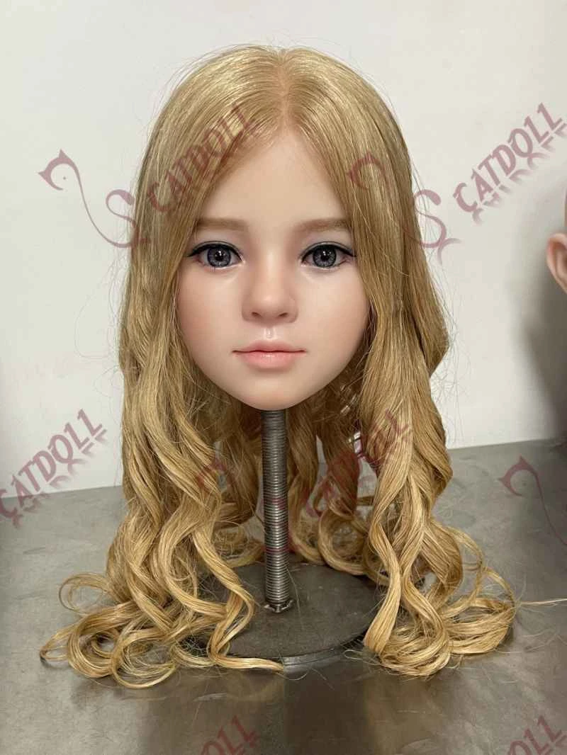
CATDOLL Ava Hybrid Silicone Head
Articles
2026-02-22
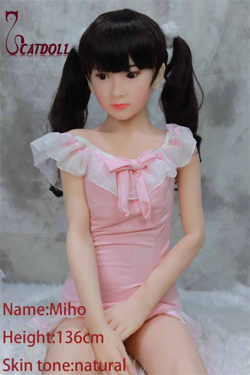
CATDOLL 136CM Miho
Articles
2026-02-22

Analysis: Latest Developments in Automotive Drive Belt Technology
Articles
2026-02-22