Read next
CATDOLL 148CM Hanako TPE
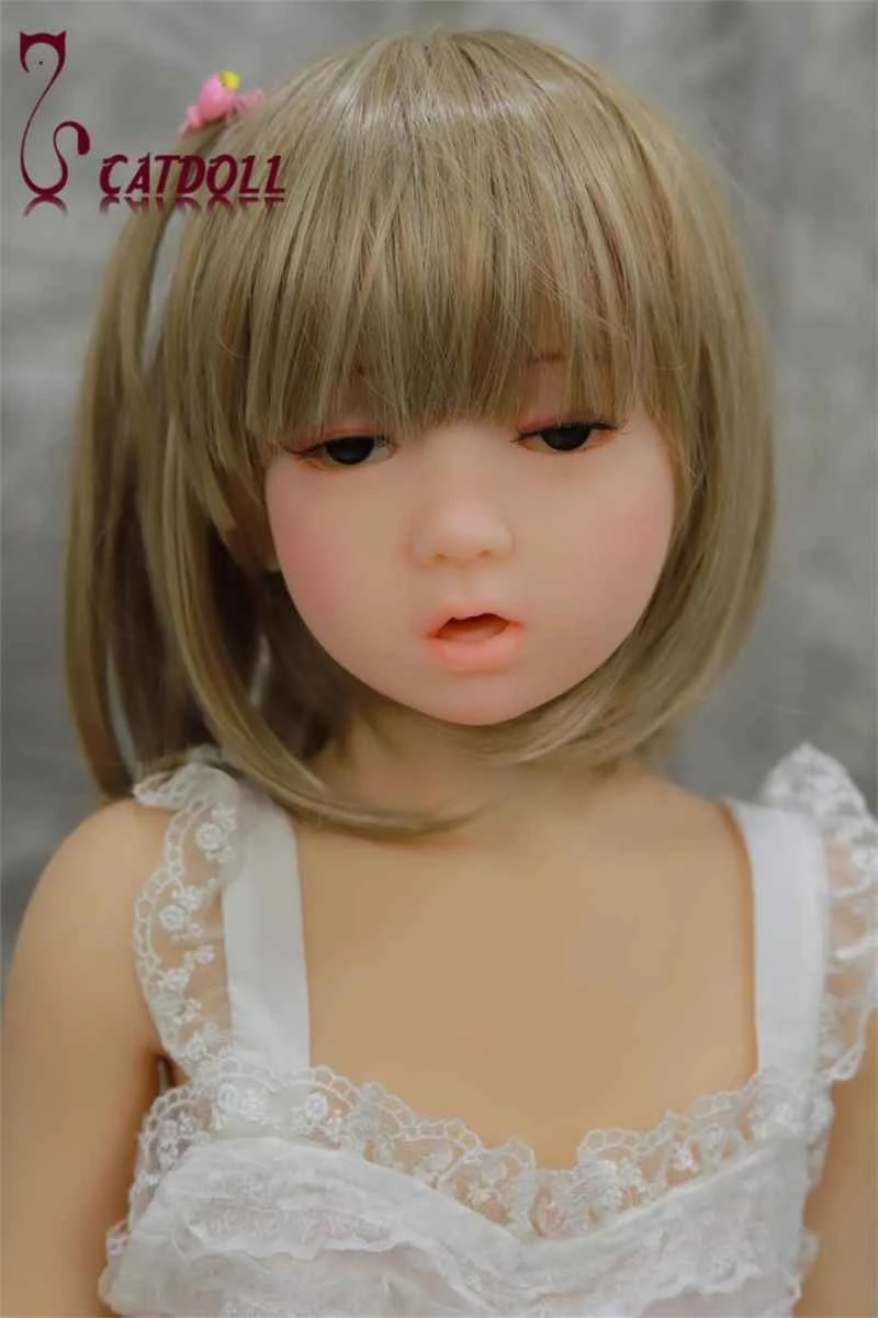
Height: 148cm Weight: 30kg Shoulder Width: 34cm Bust/Waist/Hip: 70/58/82cm Oral Depth: 3-5cm Vaginal Depth: 3-15cm Anal...
Articles
2026-02-22

CATDOLL 115CM Emelie TPE
Articles
2026-02-22

CATDOLL 139CM Lucy Silicone Doll
Articles
2026-02-22
CATDOLL EQ (Sleepy Q) 108CM
Articles
2026-02-22