Share this

FPGA-based USB 2.0 controller design

2026-04-06 08:17:24 · · #1
Abstract: This paper introduces a method for designing a USB 2.0 functional controller using VHDL, detailing its principles and design concepts, and implementing it on an FPGA. Keywords: USB, VHDL, FPGA In the fields of video storage and broadband image processing, real-time high-speed data transmission is frequently required. In April 2000, the USB 2.0 (Universal Serial Bus) transmission protocol, jointly developed by Intel, Microsoft, NEC, Compaq, Lucent, Phillips, and other companies, achieved speeds far exceeding the current 400Mbps for video transmission using the IEEE 1394 interface, reaching 480Mbps. It also boasts advantages such as plug-and-play (PnP), daisy-chaining (extension via USB hub), and the ability to connect up to 127 USB devices. This protocol can support real-time voice, audio, and video data transmission. This paper addresses the high-speed data transmission requirement by implementing a functional controller conforming to the USB 2.0 protocol specification using VHDL, enabling high-speed data transmission between the PC and peripherals in a video compression system. As shown in Figure 1, the raw video data acquired by the video A/D converter is compressed in the Philips TM1300 dedicated video processor and then sent to the PC via a USB controller. The entire process from the PC is transmitted to the TM1300 via the USB controller, decompressed, and then sent to the video D/A converter. [IMG=Video Compression System]/uploadpic/THESIS/2007/12/2007122113355051118L.jpg[/IMG] 1. Controller Structure and Principle The block diagram of the USB 2.0 controller is shown in Figure 2. The controller mainly consists of two parts: one is the interface with peripherals, and the other is the internal protocol layer logic (PL). The internal memory arbiter arbitrates the access between the internal DMA and the external bus to the memory. The PL implements USB data I/O and control. [IMG=Controller Structure Principle]/uploadpic/THESIS/2007/12/2007122113355624877F.jpg[/IMG] There are three types of interfaces: one is the functional interface with the microcontroller; one is the interface with the single-port synchronous static RAM (SSRAM); and the other is the interface with the physical layer. This conforms to the UTMI (USB Transceiver Macrocell Interface) specification definition. 2 Controller Implementation The signal block diagram of the controller interface is shown in Figure 3. The memory uses standard single-port SRAM, and its signal interface consists of a 32-bit data line SRAM_DATA, a 15-bit address line SRAM_ADDR, and read/write signals (SRAM_WE and SRAM_RD). The required SRAM capacity for the system is 215 × 32 bits = 128KB. [IMG=Controller Implementation]/uploadpic/THESIS/2007/12/2007122113360278919P.jpg[/IMG] The interface signals between the microcontroller and the microcontroller include 32-bit data lines (DATA), 18-bit address lines (ADDR), and DMA request and response signals (DMA_REQ and DMA_ACK). To support up to 128KB, 17 address lines are needed, plus one more address line to select between the SSRAM and the internal registers of the USB controller, requiring a total of 18 address lines (addr[17:0]). These are defined as follows: USB_RF_SEL <= addr[17]; USB_MEM_SEL <= addr[17]; When the 18th address bit (addr[17]) is high, the buffer memory is selected; otherwise, the internal register is selected. The address (addr[16:2]) is directly used for the address of the SSRAM memory. 2.1 UTMI Interface The UTMI interface signals include: signals related to transmitting data (TxValid, TxReady, etc.), signals related to receiving data (RxActive, RxValid, RxError, etc.), and a 16-bit bidirectional data line. At the physical layer, the controller requires an external USB transceiver; this paper uses the Philips ISP1501 chip. This chip serves as the analog front-end of USB 2.0, performing inverted non-return-to-zero (NRZI) decoding and bit-stuffing on the differential signal from the USB cable, converting it into 16-bit parallel data. Conversely, the 16-bit parallel data is serialized, bit-stuffed, and NRZI encoded through a differential driver circuit before being output to the USB cable. The ISP1501 determines the transceiver's operating mode through pins MODE0 and MODE1, with four operating modes: MODE[1:0] = "00", the transceiver is disconnected; "01" is in full speed mode (USB bandwidth is 12Mb/s); "10" is in high speed mode (USB maximum bandwidth is 480Mb/s); and "11" is in HS chirp mode. The UTMI interface controls the ISP1501's switching between HS and FS by decoding MODE[1:0]. If mode_hs='1' then MODE<='10' Elsif mode_hs='0' then MODE<='01' End if; 2.2 The core logic of the protocol layer controller is located in the PL (Protocol Layer) module, which is responsible for managing all USB data I/O and control communication. Its structure is shown in Figure 4. [IMG=USB Data I/O and Control Communication Diagram]/uploadpic/THESIS/2007/12/2007122113361371349I.jpg[/IMG] The DMA and memory interface provides random access memory and DMA operations. This module enables the PL and external microcontroller to access SSRAM using DMA. When the external bus requests access to SRAM, and the PL does not request access to memory, the control logic is as follows: req and ack correspond to the request and response signals between the external bus and memory, respectively; din, addr, and we are the data, address, and write signals given by the external bus, respectively; mreq is the request signal sent by the internal DMA to the memory; and mdin, maddr, and mwe are the data, address, and write signals given by the internal DMA, respectively. The code snippet `sel <= (req OR ack_r) AND (NOT mreq)` checks if `sel = '1' then `sram_out <= din; sram_adr <= addr; sram_we <= req AND we; else `sram_out <= mdin; sram_adr <= maddr; sram_we <= mwe; end if;` demonstrates that the internal DMA operation has a higher priority than the external bus operation. The Protocol Engine handles all standard USB handshake signals and control communications. The packet assembler assembles packets and sends them to the output FIFO, first assembling the packet header, inserting the appropriate PID (packet identifier) ​​and checksum, and then adding the data field. The packet splitter first decodes the PID, serial number, and checksum. Then, it takes the lower 4 bits (or inverts the higher 4 bits) of the 8-bit PID to obtain the PID[3:0]. It decodes the PID name using the PID type definition of the USB 2.0 protocol to determine whether it is a Token packet (OUT, IN, SOF, and SETUP) or a DATA packet (DATA0, DATA1, DATA2, and MDATA). `Pid_Token <= pid_OUT OR pid_IN OR pid_SOF OR pid_SETUP; Pid_DATA <= pid_DATA OR pid_DATA1 OR pid_DATA2 OR pid_MDATA;` If it is a Token packet (format defined as shown in Figure 5), the subsequent 16 bits of data are placed into two 8-bit temporary Token registers, token0 and token1, respectively. Then, the 7-bit address, 4-bit endpoint number, and 5-bit CRC checksum are extracted from the packet. Token_fadr<=token0[6:0]; Token_endp<=token1[2:0] & token0[7]; Token_crc5<=token1[7:3]; Special handling is required for special tokens. The controller implemented in this paper only operates on the special token SOF, and decrypts the 11-bit frame number and 5-bit CRC5 checksum after PID. Frame_no<=token1[2:0] & token0; Token_crc5<=token1[7:3]; Check if the checksum is wrong. If it is wrong, wait for the next token. Otherwise, put the address, endpoint number and frame number into the corresponding register. If the token type is IN, assemble the packet and send the packet. If it is OUT, disassemble the received data packet. Other unsupported tokens are treated as errors: Pid_ERROR <= pid_ACK OR pid_NACK OR pid_STALL OR pid_NYET OR pid_PRE OR pid_ERR OR pid_SPLIT OR pid_PING; if an error occurs, the token is not decoded, and the system waits for the next token. If it is a DATA packet, the PID is followed by a maximum payload of 1024 bytes of data and a 16-bit CRC16 checksum. Data processing involves first writing to the endpoint register, and then writing to SSRAM via DMA operation. The endpoint register and DMA operation are described in detail below. 2.3 Endpoint Operation Data transmission is actually performed through the endpoint. The controller configures the endpoint by writing to the endpoint register. The controller can have up to 16 endpoints, each with four corresponding registers: Epn_CSR, Epn_INT, Epn_BUF0, and Epn_BUF1 (where n = 0, 1, 2, or 3), as shown in Figure 6. This article uses addr[8:2]7 to access these registers via address lines, and addr[8:4] to select the endpoint number, whose values ​​(hexadecimal) from 4 to 19 represent Epn (n=0...15). addr[3:2] specifies the register type: "00" represents CSR (Control Status Register); "01" represents the interrupt register; "10" points to Buffer0; "11" represents Buffer1. These two buffers are used for temporary data storage, and Buffer0 and Buffer1 are used as dedicated input/output buffers to improve the data throughput of USB. Dual buffers can reduce the latency between the microcontroller and the driver software. The endpoint's CSR register specifies the endpoint's operating mode and reports the status of the specified endpoint to the controller. Ep_CSR[31:30] must be initialized to "00" (initially using Buffer0), and by reading these two bits, the next buffer to be processed can be determined; when it is "01", Buffer1 is specified. Ep_CSR[27:26] and Ep_CSR[25:24] specify the endpoint type and transfer type, respectively. Their type encoding is shown in Table 1. Ep_CSR[21:18] specifies the endpoint number, and there can be a total of 16 endpoints. Ep_CSR[15] is the DMA enable bit. When it is "1", external DMA operation is allowed; otherwise, DMA operation is not allowed. [IMG=Endpoint Operation]/uploadpic/THESIS/2007/12/20071221133619577925.jpg[/IMG] When the controller receives an interrupt, it reads the interrupt source register (Ep_INT[6:0]) to determine the interrupt source and the cause of the interrupt. The interrupt source can be customized. For example, Ep_INT[2] is defined as the interrupt generated when the controller receives an unsupported PID: Ep_INT[2]<=Pid_ERROR. Ep_INT[4] and Ep_INT[3] represent the full or empty status bits of Buffer1 and Buffer0, respectively. Ep_BUF[31] (marks whether the buffer has been used) is set to "1" by the controller after use, and cleared by the controller after the buffer is emptied or refilled. The buffer is initialized to "0". Ep_BUF[30:17] specifies the number of bytes the buffer can hold. Ep_BUF[16:0] is a pointer to the buffer, the address of the data loaded in the SRAM memory. The control endpoint (Endpoint0) is special because it needs to both receive and send data. Therefore, for the control endpoint, Buffer0 is used as the OUT buffer, and Buffer1 is the IN buffer. Data from SETUP and OUT groups is written to Buffer0, and data from IN groups is obtained from Buffer1. [IMG=Data from SETUP and OUT groups]/uploadpic/THESIS/2007/12/2007122113363062906R.jpg[/IMG] 2.4 DMA Operation DMA operation allows transparent data transfer between the controller and the functional interface. Once DMA operation is set up, no microcontroller intervention is required. Each endpoint has a pair of DMA_REQ and DMA_ACK signals. When the DMA enable signal bit (Ep_CSR[15]) in the CSR register is set, the USB controller uses the two signals DMA_REQ and DMA_ACK to perform DMA flow control. When the buffer has data or is empty and needs to be filled, a DMA request signal DMA_REQ is sent. A DMA_ACK signal is responded to for every 4 bytes transferred. Since the transaction operation defined by the USB2.0 protocol is in 8-bit units, it takes 4 writes of 8 bits to complete a 32-bit DMA operation. The internal DMA adopts an efficient one-hot state machine design method, and the state transition is shown in Figure 7. When it is necessary to store the received data into SRAM (rx_dma_en=1), it enters the WAIT_MRD state. In this state, a temporary data register is selected, and a request signal mreq is sent to the memory. 4 bytes are prefetched from the memory (when the received data is less than 4 bytes, it is guaranteed that 4 bytes of data are written to the memory) into the register, and then it enters the MEM_WR state. When the PL's packet splitter receives 1 byte of data, it writes the byte to temporary memory and transitions to the next state, MEM_WR1. When the packet splitter has no data to send to the DMA arbiter, it enters the MEM_WR2 state, where it writes the data from the temporary memory to SRAM and then returns to the IDLE state. During operation, a counter, adr_cb, is used to count the number of bytes transmitted. The value of addr_cb[1:0] indicates which byte of the 32-bit sequence is currently being transmitted. The counter sizu_c increments by 1 for each byte received. When data needs to be read from SRAM (tx_dma_en=1), the DMA arbiter enters the MEM_RD1 state from the IDLE state, reads 4 bytes of data into the transmit buffer, then enters the MEM_RD2 state, and then reads 4 bytes into the MEM_RD3 state. These 8 bytes take turns using the Buffer0 and Buffer1 buffers: When data needs to be read from SRAM (tx_dma_en=1), the DMA arbiter enters the MEM_RD1 state from the IDLE state, reads 4 bytes of data into the transmit buffer, then enters the MEM_RD2 state, and then reads 4 bytes into the MEM_RD3 state. These 8 bytes take turns using the Buffer0 and Buffer1 buffers: if ((NOT adr_cb[2]) AND mack then Buffer0<=SRAM_DATA_I; elsif (adr_cb[2] AND mack) then Buffer1<=SRAM_DATA_I; end if; In the MEM_RD3 state, it determines whether more data needs to be read. If so, it enters the MEM_RD2 state; otherwise, it returns to the IDLE state after all bytes have been transmitted. During data transmission, a 14-bit counter sizd_c, taken from Ep_BUF[30:17], is used to determine the number of bytes transmitted. Its value is decremented by 1 for each byte transmitted. In each state shown in Figure 7, the Abort signal generated by the PE will cause the current state to return to IDLE if there is a timeout, CRC check error, or incorrect data. Conclusion This paper describes an implementation scheme for a USB 2.0 function controller. Its VHDL implementation code has been tested and approved by Xilinx on the XILINX FPGA Virtex XVV3006fg456. ISE simulation, synthesis, and placement/routing. The FPGA has 320,000 gates and 1536 CLBs (Configurable Logic Units). The control module occupies 2050 slices (66%), uses 1697 slice flip-flops (27%), and 3047 4-input LUT tables (49%). The entire FPGA can reach a speed of 56.870MHz, fully meeting the high-speed transmission requirements of video data (for 32-bit data operations, a clock speed of 480Mb/s is achieved with only 15MHz). The controller implemented in this scheme is easy to modify and implement, and can be embedded into the SOC as a functional module, allowing for maximum flexibility in designing the on-chip system for different situations.
Read next

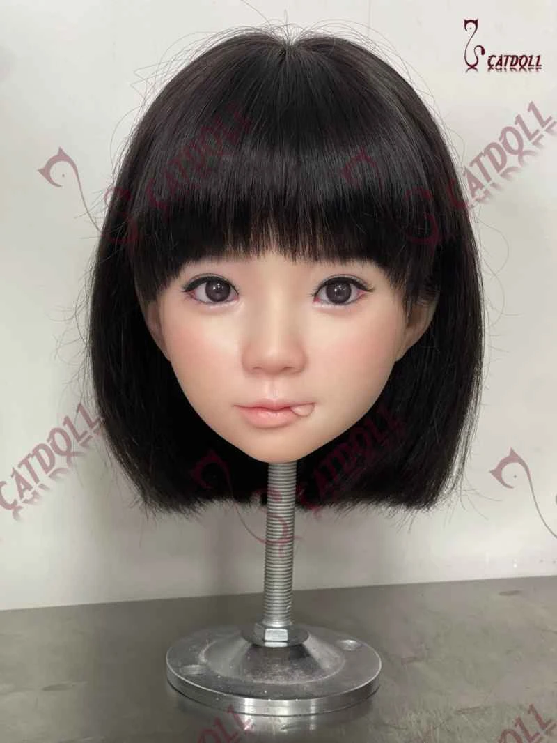
CATDOLL 88CM Maruko (soft Silicone Head with TPE Body)

Height: 88cm Weight: 11.5kg Shoulder Width: 25cm Bust/Waist/Hip: 49/45/51cm Oral Depth: 3-5cm Vaginal Depth: 3-13cm Anal...

Articles 2026-02-22