Read next
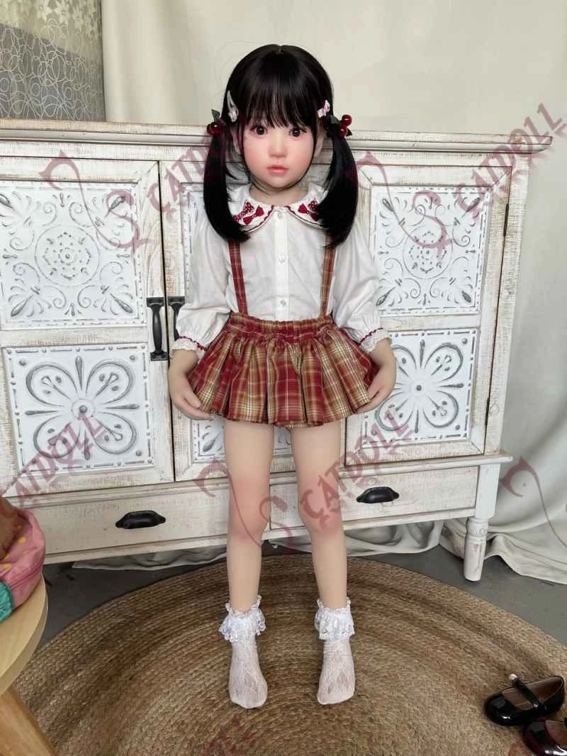
CATDOLL 130CM Nanako (Customer Photos)
Height: 130cm Weight: 27kg Shoulder Width: 31cm Bust/Waist/Hip: 64/60/72cm Oral Depth: 3-5cm Vaginal Depth: 3-15cm Anal...
Articles
2026-02-22

CATDOLL 138CM Yoyo (TPE Body with Soft Silicone Head)
Articles
2026-02-22
CATDOLL Nanako 109CM TPE (Soft Silicone Head with Pale Tone)
Articles
2026-02-22
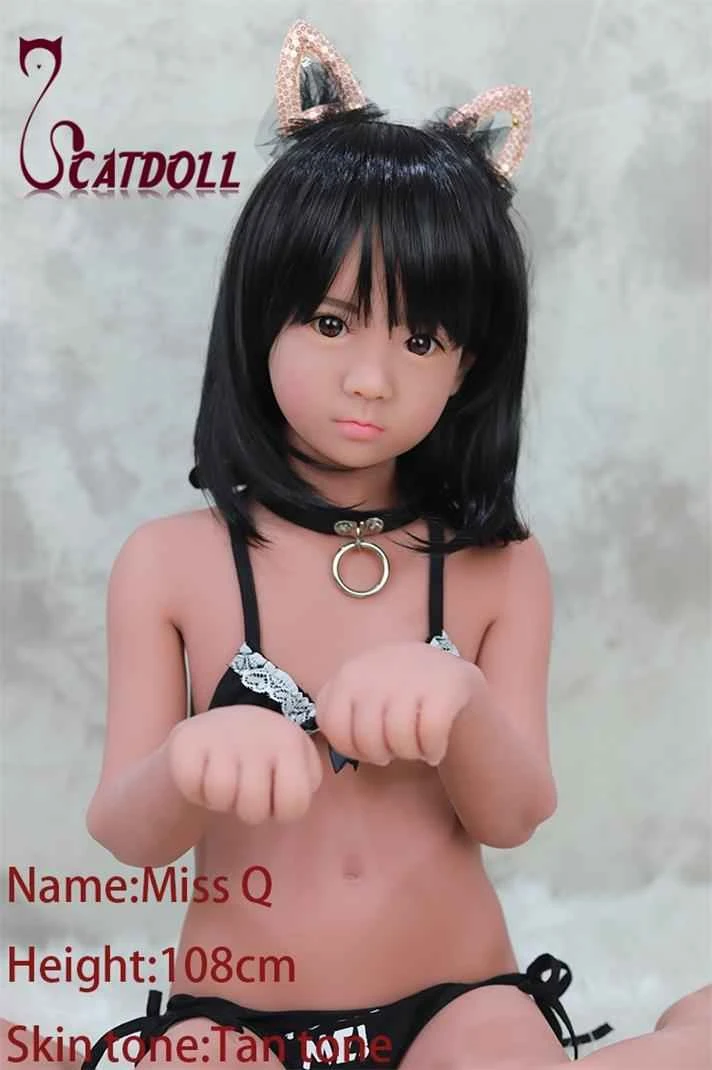
CATDOLL Q 108cm Tan Tone
Articles
2026-02-22