Read next
CATDOLL 128CM Kiki (TPE Body with Hard Silicone Head)
Height: 128cm Weight: 19kg Shoulder Width: 30cm Bust/Waist/Hip: 57/52/63cm Oral Depth: 3-5cm Vaginal Depth: 3-15cm Anal...
Articles
2026-02-22

CATDOLL 148CM Hanako Silicone Doll
Articles
2026-02-22
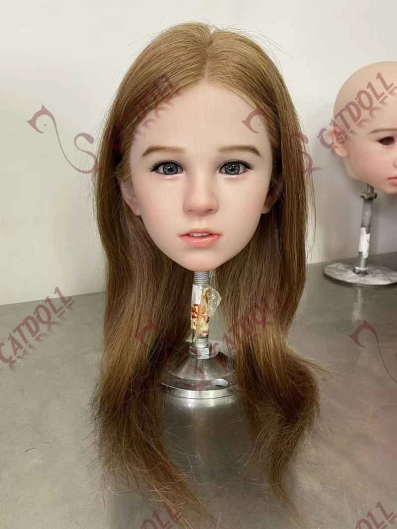
CATDOLL Dolly Hybrid Silicone Head
Articles
2026-02-22

Human-Machine Interface Prototyping Strategies for Embedded Systems
Articles
2026-02-22