Read next
CATDOLL 126CM Laura
Height: 126cm Weight: 23kg Shoulder Width: 32cm Bust/Waist/Hip: 61/58/66cm Oral Depth: 3-5cm Vaginal Depth: 3-15cm Anal...
Articles
2026-02-22

CATDOLL 115CM Momoko TPE
Articles
2026-02-22
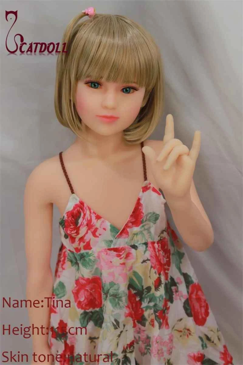
CATDOLL CATDOLL 115CM Tina TPE
Articles
2026-02-22

CATDOLL 126CM Nanako
Articles
2026-02-22