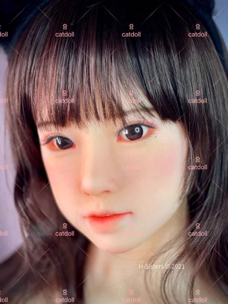
Design of a smart transmitter based on the HART protocol
2026-04-06 07:31:07··#1
Abstract: Starting from the functions and protocol requirements of HART protocol intelligent pressure/differential pressure transmitters, this paper discusses and analyzes the design focus, difficulties, and key technologies of HART protocol intelligent transmitters in detail, and designs a complete practical circuit for a HART protocol intelligent pressure/differential pressure transmitter. It can realize the basic functions of a HART protocol intelligent transmitter. Keywords: HART protocol, intelligent transmitter, fieldbus, digital data communication . Fieldbus technology is currently one of the hot topics in automatic detection technology. From the perspective of its formation, fieldbus technology is an inevitable result of the development of control, computer, communication, and network technologies; while intelligent instruments have laid the foundation for the emergence and application of fieldbus. Since Honeywell launched the Smar transmitter in 1983, various manufacturers worldwide have successively launched their own unique intelligent instruments. To solve the problem of sharing open resources, both users and manufacturers strongly demand the formation of a unified standard to promote the formation of fieldbus technology. Currently, several influential fieldbus technologies include: Foundation Fieldbus, LonWorks, PROFIBUS, CAN, and HART. Except for HART, all are fully digital fieldbus protocols. Full digitalization means eliminating traditional analog signal transmission methods and requiring each field device to have intelligent and digital communication capabilities. This allows operators or other devices (sensors, actuators, etc.) to send commands (such as setpoints, ranges, alarm values, etc.) to the field, while simultaneously receiving real-time information on various aspects of the field devices (such as measured values, environmental parameters, equipment operating status, equipment calibration, self-diagnostic status, alarm information, fault data, etc.). Furthermore, control calculations previously performed by the main controller are distributed across various field devices, significantly improving system reliability and flexibility. A key aspect of fieldbus technology is its openness, emphasizing consensus and adherence to standards. This breaks down the traditional situation of independent standards from different manufacturers, ensuring that products from different manufacturers can be integrated into the same fieldbus system and share resources with other systems through gateways. Currently, while fieldbus standards are still under development and refinement, traditional 4-20mA analog devices are still widely used in various fields of industrial control. Therefore, immediate full digitalization is unrealistic. To meet the transition from analog to full digital, the HART protocol was developed. HART employs Frequency Shift Keying (FSK) technology. Based on the Bell202 communication standard, it transmits digital signals by superimposing different frequency signals (2200Hz represents "0", 1200Hz represents "1") onto a 4-20mA analog signal (see Figure 3). The HART protocol has a data transmission rate of 1200bps (bits/second). The HART fieldbus (HF) system adopts a master-slave working mode: the master is one IBM-PC; the slave is one or more HF smart transmitters that comply with the HART protocol. When there is only one HF smart transmitter as a slave, i.e., the smart transmitter is operating in point-to-point mode, the traditional 4-20mA signal can continue to be used for analog transmission, while measurement, adjustment, and test data are transmitted digitally. When there are multiple HF smart transmitters as slaves, i.e., the smart transmitters are operating in multi-station mode, the 4-20mA signal is discarded, and each transmitter operates at a current of approximately 4mA. All measurement, adjustment, and test data are transmitted digitally. Because each HF transmitter has a unique serial number, the host computer can operate on each transmitter. HART provides a Device Description Language (DDL) to ensure interoperability. It should be noted that while HART is considered a de facto industry standard, it is not a true fieldbus (a hybrid of analog and digital); it is merely a prototype and a transitional protocol. Since the 4–20mA analog signal standard will exist for a considerable period, research on the HART protocol remains significant. This paper discusses the technical issues of hardware implementation for HART protocol-based intelligent transmitters. Firstly, it addresses the issue of low power consumption; secondly, it discusses effective methods for implementing the communication functions of HART protocol intelligent transmitters. I. Power Consumption Requirements To achieve the basic functions of an intelligent transmitter, such as linearization, temperature compensation, automatic zero-point and range adjustment, and digital communication, the following key components are necessary: microcontroller, A/D converter, D/A converter, communication chip, and sensor. Figure 1 is a block diagram of a HART protocol intelligent transmitter. The analog signal from the sensor is converted into a digital signal by an A/D converter and then sent to the microcontroller. The microcontroller processes the digital signal and outputs a 4-20mA standard current signal via a D/A converter and a V/I conversion circuit. During digital communication, the microprocessor transmits and receives data through a communication interface chip and coupling circuit, using a 4-20mA current loop as the medium. The memory in Figure 1 stores the sensor's characteristic parameters, field commands, field status, and other operating parameters. The core is a Bell 202 communication standard HART modem, with waveform shaping and bandpass filters added at both the output and input ends to enhance communication reliability. 1. Power Consumption Requirements To be compatible with the current 4-20mA standard, the HART protocol smart transmitter must be able to operate in a 4-20mA two-wire loop. This means that the current available to power the transmitter cannot exceed 4mA. In practical applications, to ensure compatibility with both digital and analog signals, the data frequency signal is typically converted into a ±0.5mA frequency signal via the regulating transistor of a V/I conversion circuit. This signal is then superimposed on a 4–20mA current loop across the two lines (2200Hz represents "0", 1200Hz represents "1"). Due to the characteristics of the signal, the average value of this signal is 0, thus the analog and digital signals do not interfere with each other. However, the instantaneous maximum current in the loop is I = 4.5mA, and the minimum is I = 3.5mA. If too much power is supplied to the transmitter, exceeding 3.5mA, it will cause distortion in the negative half-cycle of the digital signal. Considering the margin required for adjustment, it is advisable that the power supply current to the transmitter generally should not exceed 3.4mA. 2. Power Supply Methods There are two main ways to power the transmitter system: One is to directly regulate the input voltage to the required voltage (5V or 3.3V) before supplying power to the system. In this method, the total current must be controlled within 4mA. The second is to use a DC-DC power supply. As long as the efficiency of the DC-DC converter is high enough, it is much more lenient in terms of power consumption control than the first method. However, the negative impact of the converter's linear stability factors must be considered. Due to the emergence of low-power, cost-effective integrated circuits, the first method is more advantageous because both methods require consideration of voltage adaptability. Industrial sites typically use DC 24V, but DC 36V is also used. Transmitters are generally required to operate stably and reliably under DC 12-42V supply voltages. In this respect, direct power supply is much more flexible than DC-DC conversion. II. Communication System 1. Communication Chip: The HT2012, manufactured by SMAR, is a Bell 202 standard single-chip microcontroller CMOS low-power FSK modem. It is a dedicated chip for providing HART communication functions in the design of process control instruments and other low-power equipment. The HT2012 consists of four main functional modules: clock frequency, demodulator, modulator, and carrier detection. The HT2012 requires an external clock input of 460.8kHz, a 3-5V power supply, and low power consumption (typical 40μA) [5]. The HT2012 modem is half-duplex. When one is running, the other of the modulator and demodulator will be stopped. It operates on the Bell 202 standard, with a transmit, transmit, and receive modulation bit rate of 1200bps. The HT2012 uses 1200Hz ("1") and 2200Hz ("0") Bell 202 signal frequencies and is CMOS and TTL compatible. The HT2012 has a carrier detection output terminal OCD, which is active low, indicating that the other communication chip is ready to transmit a carrier, improving the real-time performance and flexibility of communication. In addition, the 19.2kHz clock signal output also provides convenience for applications. 2. D/A and V/I Converters To convert digital frequency signals into ±0.5mA frequency signals superimposed on a 4-20mA current loop across two lines, additional coupling circuitry is required, inevitably leading to increased power consumption. However, the AD421 from Analog Devices (A/D) is a 16-bit D/A converter specifically designed for HART protocol smart instruments, including a 4-20mA current loop. It is HART protocol compatible, and its switching current source and filter function blocks can convert HART voltage signals to ±0.5mA current signals, facilitating applications. AD421 basic performance: (1) 4-20mA output; (2) HART compatible, capable of standard HART FSK protocol communication; (3) 16-bit resolution; (4) ±0.01% integral nonlinearity; (5) 3V, 3.3V or 5V adjustable voltage output and 2.5V and 1.25V accuracy references for itself and other system devices; (6) 750μA maximum quiescent current when powered by Vcc=5V, with a typical value of 575μA; (7) Programmable alarm current function, allowing the transmitter to issue an out-of-range current alarm to indicate a converter fault; (8) Flexible high-speed serial interface. The AD421 has two operating modes: 4-20mA output mode and 3.5-24mA alarm output mode. III. Microcontroller and A/D Converter1. A/D Converter To realize the functions of an intelligent transmitter, the circuit hardware design requires an adjustable-gain instrumentation amplifier and an A/D converter with a resolution of at least 14 bits to amplify and convert the sensor signal from analog to digital. This is necessary to meet the design requirements of high precision, automatic range adjustment, and large range ratio of the intelligent transmitter. For intelligent differential pressure transmitters, static pressure and temperature sampling is also required to achieve static pressure and temperature compensation and improve measurement accuracy across the entire range. This necessitates a multiplexer to switch between channels. If discrete components are used, significant power consumption will inevitably be introduced, making it difficult to meet the power consumption requirements of HART protocol intelligent transmitters. Some large companies have designed dedicated A/D converters compatible with 4-20mA intelligent transmitters, such as MAXIM's MAX1400 and Analog Devices' AD7714. Their common feature is that they integrate an adjustable gain instrumentation amplifier, multiplexer and A/D converter into one chip with a power consumption of about several hundred μA, which makes it convenient to realize HART protocol intelligent transmission. MAX1400 basic performance: (1) MAX1400[1] is a low power, multi-channel ∑/Δ A/D converter with SPI synchronous serial port; (2) 18-bit resolution; (3) 3 fully differential or 5 quasi-differential signal input channels; (4) Programmable PGA, with selected gains of (1, 2, 4, 8, 16, 32, 64 or 128); (5) AIN1~AIN6 can form 3 fully differential input channels or 5 quasi-differential input channels; (6) 2 additional fully differential system correction channels CALOFF and CALGAIN are used for offset and gain error correction; (7) 2 drift compensation buffers in MAX1400 are used to isolate the selected input from the capacitive load of PGA and modulator. When V+ is powered by 5V, the reference input of MAX1400 is 2.5V, and the range of analog input variation is -Vimax to +Vimax. Vimax = 5 ÷ (2 × GAIN). 2. Microcontroller To realize a high-performance, low-power intelligent transmitter control circuit, the microcontroller selected is PIC16C73[7]. It has the characteristics of low power consumption, fast running speed and strong power consumption. It adopts long byte instructions, all instructions are single word length, except for jump to double cycle instructions, all are single cycle (4 clock cycles) instructions. It contains a watchdog, 8-level hardware stack, 192×8 RAM, 32-bit timer, 2 captures, 5-channel 8-bit A/D converter, synchronous serial port shared by SPI/I2, 1 asynchronous transmit/receive serial port USART, and multiple interrupt functions, including B port RB4~RB7 input level change interrupt. IV. Design of a Smart Pressure/Differential Pressure Transmitter Based on HART Protocol The integrated circuits used in the circuit are those mentioned above, characterized by high integration, good cost-performance ratio, low power consumption, and powerful functionality. Inter-chip data communication uses the Motorola Serial Peripheral Interface (SPI), which has the advantages of low MCU resource consumption and expandability according to system size. In practical applications, the microcontroller can be easily connected to integrated circuit chips with SPI interfaces, such as A/D, D/A converters, and data memory. Since the PIC16C73 microcontroller has an SPI serial bus hardware interface, data communication speed is higher and its use is more flexible. 1. Circuit Description: The two fully differential channels AIN1, AIN2 and AIN3, AIN4 of the MAX1400 A/D converter perform digital conversion on the differential pressure sensor TRS1 and the static pressure sensor TRS2, respectively. AIN5 and AIN6 form a quasi-differential input channel to monitor the constant current input of TRS1. All sensors are semiconductor piezoresistive sensors. A characteristic of piezoresistive sensors is that each bridge arm has a relatively large resistance, typically 2kΩ. The following assumes a bridge arm resistance of 2kΩ. Constant current power supply further reduces the sensor's nonlinearity and the impact of temperature on the sensor's output sensitivity. Experiments show that the change in the equivalent resistance of pressure and differential pressure sensors over the entire temperature range (0–70℃) is approximately 100 times the change in equivalent resistance caused by pressure or differential pressure across the entire range. Therefore, the A/D value measured by AIN5 can provide temperature compensation for the entire transmitter. To improve the transmitter's measurement accuracy, the error caused by static pressure to the differential pressure must be compensated. Therefore, fully differential channels AIN3 and AIN4 are designed in the circuit to monitor the static pressure sensor TRS2, thereby achieving static pressure compensation. The HART communication module consists of an HT2012, waveform shaping circuit, and bandpass filter. The shaping resistors consist of 74HC126 (four tri-state output buffers) and, through two 750Ω resistors and a 2.2μF coupling capacitor, input the shaped voltage signal from the HT2012 to the switching current source and filter function block of the AD421, enabling the conversion of the HART voltage signal from a ±0.5mA current signal. The bandpass filter consists of the two operational amplifiers, resistors, and capacitors shown in the thin box in Figure 4. It converts the ±0.5mA HART current signal in the 4–20mA loop into a HART voltage signal, which is then demodulated by the HT2012 and sent to the microcontroller's serial communication interface to complete the data reception task. In addition to outputting the 4–20mA current signal and handling HART communication, the AD421 also provides power and a reference voltage for the system. Its 2.5V reference voltage is used by itself and the MAX1400. The data memory uses a 24LC65, an 8KB serial E2PROM, with a power supply voltage of 2.5–5.5V and power consumption: read current 150μA; write current 3mA (5V power supply). It stores sensor characteristic parameters, field configuration commands, operating parameters, and communication data. The 19.2kHz signal from the HT2012 is sent to the counter input of the PIC16C73 to detect the HT2012's operating status. The OCD signal from the HT2012 is sent to the RB7 pin of the PIC16C73. RB7 is set to interrupt mode for detecting communication status. 2. Power Consumption and Current Distribution: The AD421 is powered by a 4–20mA loop main power supply. The converted 5V power supply powers itself, the 24LC65, and the analog circuitry of the MAX1400. A power consumption margin must be included in the design. The AD421 operates at a current of 600μA, the 24LC65 reads at 10μA, and the MAX1400's analog circuit operates at a current not exceeding 100μA. The transmitter's power consumption is designed to be 3.4mA, leaving 2.5mA for other components in the circuit. The specific allocation is as follows: the sensor is powered by a 0.5mA constant current diode (3CRC), and the remaining 2.0mA is supplied by another 3CRC diode for other parts of the circuit. This avoids the 4-20mA signal variation caused by differences in power consumption between dynamic and static operation (although experiments show this variation is very small). The 3CRC constant current principle is as follows: it internally provides a stable 1.24V, which is led out from two pins. Connecting a resistor to these two pins provides the constant current output. The calculation formula is: I (mA) = 1.24/R (kΩ). As long as the 3CRC's operating voltage is slightly greater than 1.24V, it will operate normally. A ZRC330 Zener diode is selected. Its regulated voltage is 3.3V, minimum operating current is 20μA, maximum absorption current reaches 5mA, and temperature coefficient is 50ppm, making it a relatively ideal device. The MAX1400's operating current is less than 150μA (3.3V supply), the HT2012's power dissipation current is 40μA, and the bandpass filter uses the TLC27L2C op-amp, with a maximum power dissipation current of only 48μA. The 74HC126 shaping circuit operates at a maximum current of approximately 500μA at low frequencies, leaving 1.25mA for the microcontroller. The PIC16C73 microcontroller's power consumption is 2.0mA at a 4MHz clock and Vdd=3V; while at 4MHz and 20MHz clocks and VDD=5V, the current values are 2.7mA and 13.5mA, respectively. It is evident that appropriately reducing the microcontroller's operating frequency can significantly reduce its power consumption. Since all instructions of the PIC16C73 except for jump instructions are single-byte instructions, the instruction cycle is only 4 clock cycles. Its running speed is faster than other types of microcontrollers. Appropriately reducing the working frequency still makes its running speed far meet the real-time requirements of the transmitter. The microcontroller in this design uses a working frequency of 1MHz, and its power consumption experimental data is less than 1mA. The main working clock of HT2012 is a special 460.8kHz, which needs to be obtained from SMAR. This circuit uses one PIC16C58A[7] microcontroller, connected to an external 1.8432MHz crystal oscillator. After the microcontroller divides the frequency by 4, it outputs a clock of 460.8kHz, which is directly used by HT2012. The PIC16C58A microcontroller is a low-end product in the PIC series of microcontrollers, and its power consumption is comparable to that of the PIC16C73. Since the circuit has added one microcontroller, the power consumption of the entire circuit will exceed the allowable range. To ensure power consumption, the circuit design employs a time-division multiplexing method: the program uses V1, V2, and V3 to implement time-division multiplexing between the sensor and the PIC16C58A. When the transmitter is performing A/D conversion, the system powers the sensor. When communication needs to be detected or actively initiated, the microcontroller shuts off the 0.5mA supply to the sensor and connects the current to the 3.3V operating power supply, simultaneously activating the PIC16C58A. The PIC16C58A's power consumption specification is less than 15μA at a 32kHz clock speed and VDD=3V. Because a specific I/O port (such as RB) of the PIC16C58A can be set high or low, there is no risk of program crashes. Therefore, the on-chip WDT function of the PIC16C58A is not needed; setting it to OFF significantly reduces power consumption. Thus, the PIC16C58A's power consumption will not exceed 0.5mA when operating at a 1.8432MHz clock speed. Regarding the power consumption of the 24LC65 data memory: the read current is 150μA, which is not a power consumption issue; however, the write current is 3mA, which generally occurs for a short period after data communication is completed. This power consumption requirement can be resolved by specifying that the 4-20mA current signal is invalidated during communication. The 24LC65 must be connected to a 4-20mA main power supply. Based on the above analysis, a smart transmitter with a power consumption of less than 3.4mA meets the requirements. Conclusion This paper starts from the basic functions of a smart transmitter and, considering the characteristics of data communication and power consumption requirements of HART protocol smart transmitters, designs an application circuit for a smart pressure/differential pressure transmitter based on extensive experiments. The MAX1400, AD421, and HT2012 all passed program debugging. This circuit uses only one pressure sensor, which is a pressure transmitter. If the pressure sensor is replaced with a temperature sensor, it becomes a HART protocol smart temperature transmitter. Due to limitations in expertise, there are bound to be many areas for improvement in this paper. It is hoped that this research can provide helpful assistance to the development of smart transmitters.