Read next
CATDOLL 115CM Kiki TPE
Height: 115cm Weight: 19.5kg Shoulder Width: 29cm Bust/Waist/Hip: 57/53/64cm Oral Depth: 3-5cm Vaginal Depth: 3-15cm An...
Articles
2026-02-22
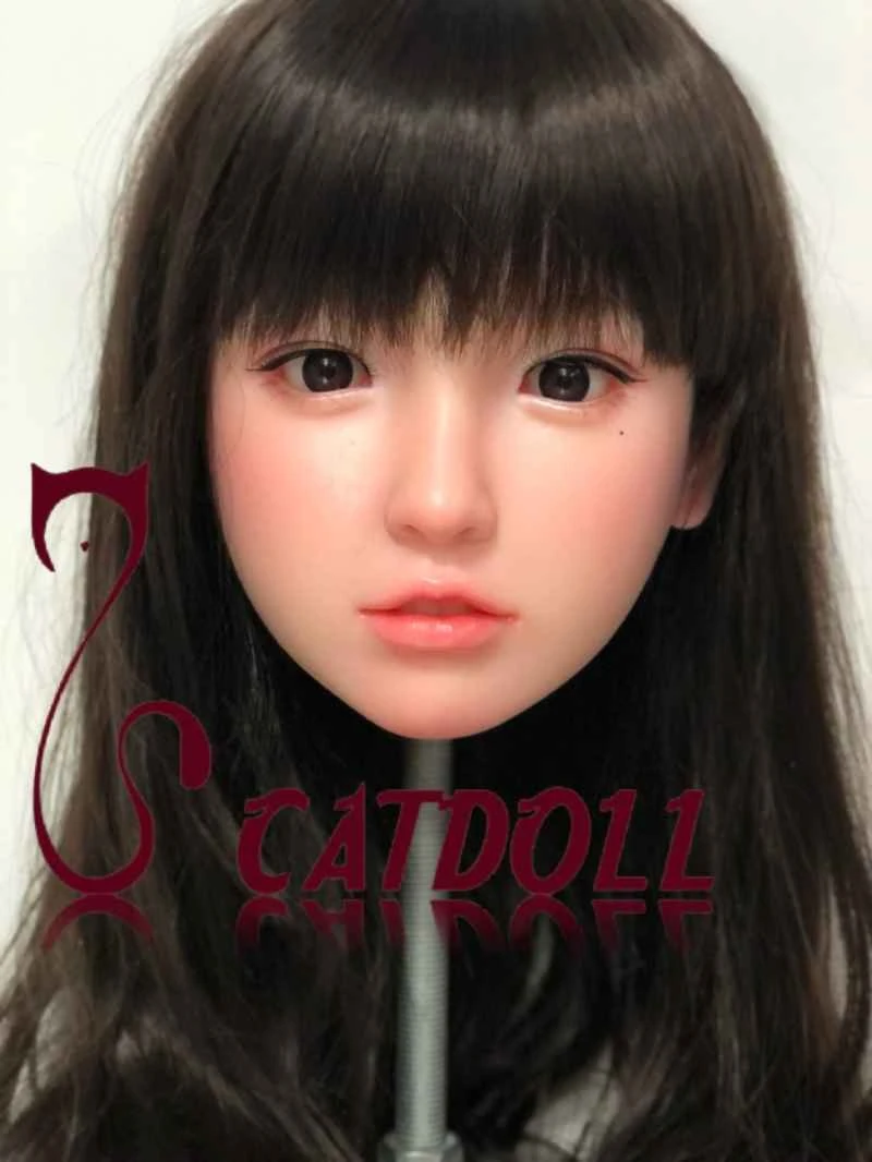
CATDOLL Hanako Soft Silicone Head
Articles
2026-02-22

CATDOLL Q 108cm Natural Tone – Customer's Photos
Articles
2026-02-22

CATDOLL 135CM Vivian
Articles
2026-02-22