Read next
CAN Interface Design of Smart Instruments
Abstract: Currently, there are more than a dozen types of fieldbuses, each with different specifications and applicable ...
Articles
2026-02-22

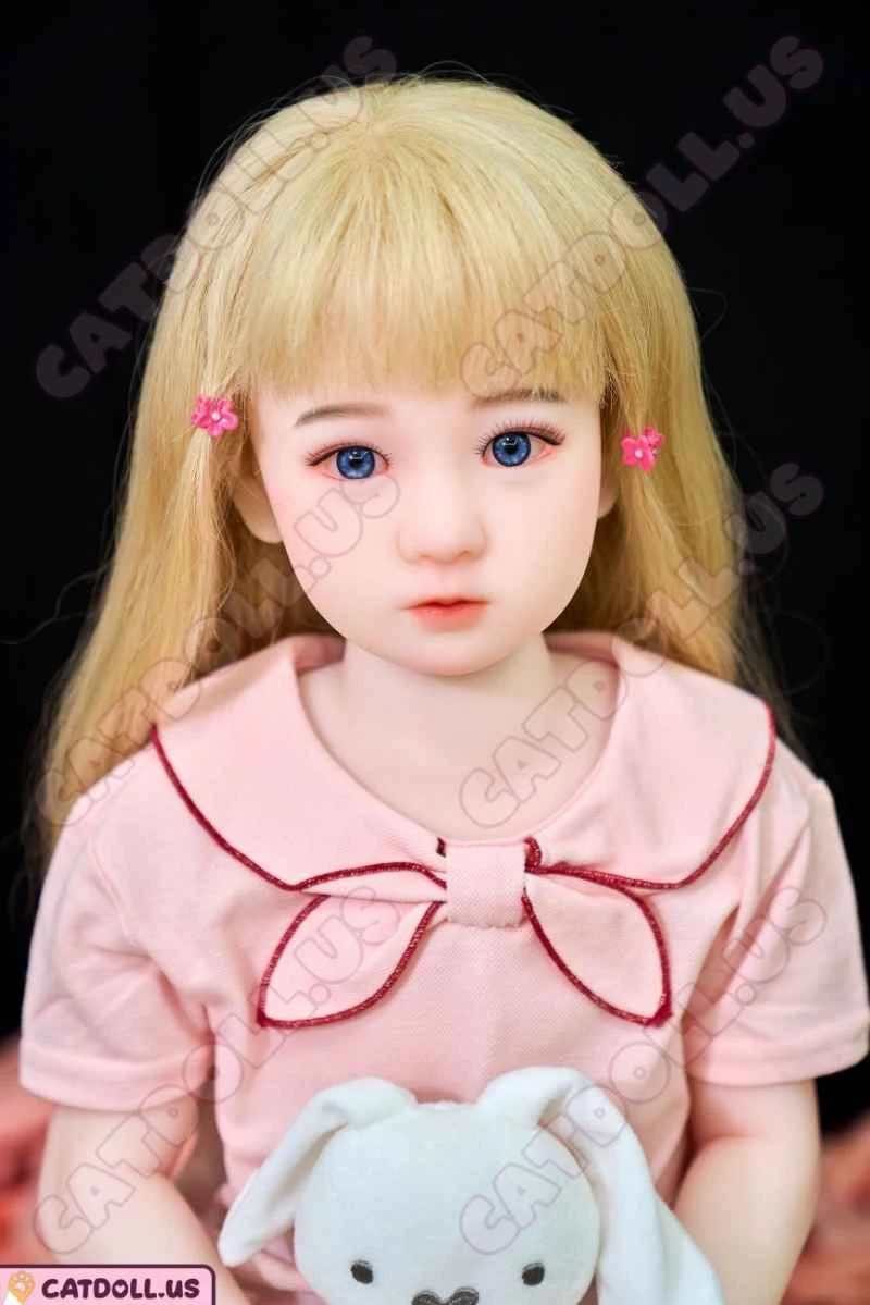
CATDOLL Mimi Hard Silicone Head
Articles
2026-02-22
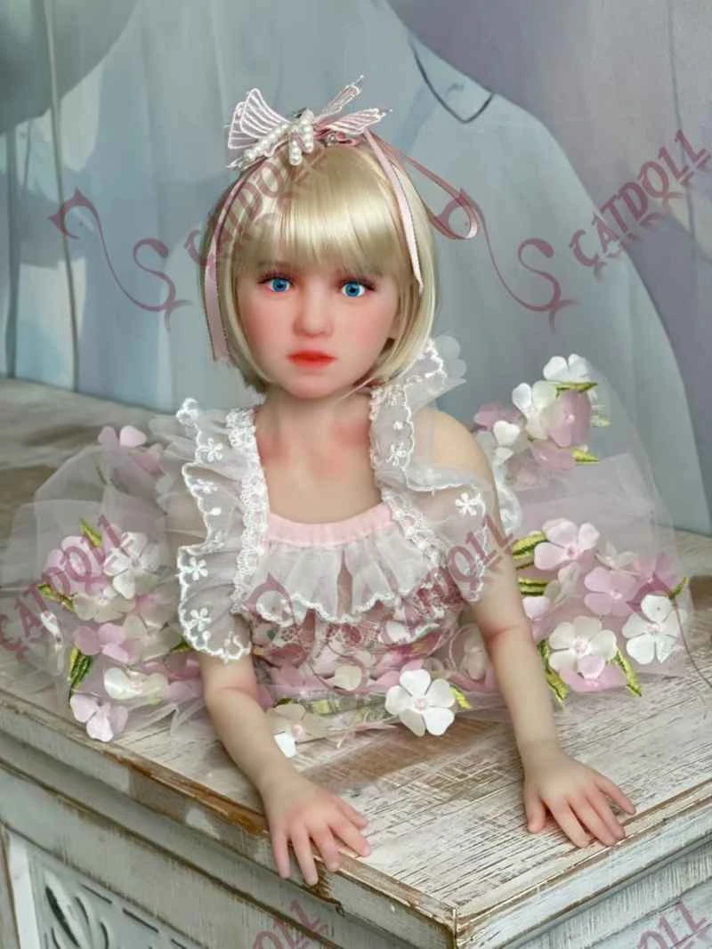
CATDOLL Q 88CM TPE Doll
Articles
2026-02-22
CATDOLL Sasha 60cm – Soft TPE Petite Body
Articles
2026-02-22