Read next
CATDOLL 146CM Laura TPE
Height: 146cm A-cup Weight: 26kg Shoulder Width: 32cm Bust/Waist/Hip: 64/54/74cm Oral Depth: 3-5cm Vaginal Depth: 3-15c...
Articles
2026-02-22
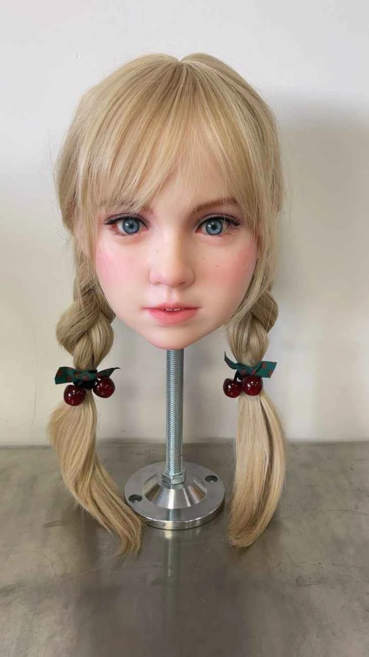
CATDOLL Sasha Soft Silicone Head
Articles
2026-02-22
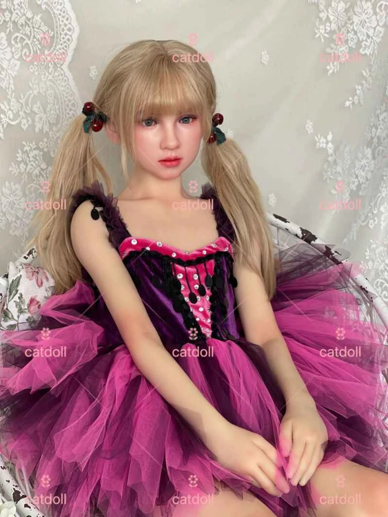
CATDOLL 139CM Charlotte (TPE Body with Soft Silicone Head)
Articles
2026-02-22
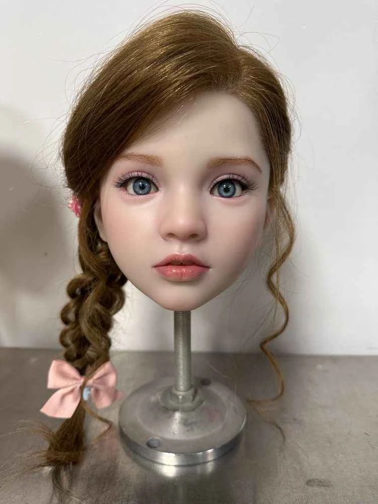
CATDOLL Milana Hard Silicone Head
Articles
2026-02-22