Read next
CATDOLL 92CM Shota Doll Q (Male Doll)
Height: 92cm Male Weight: 13kg Shoulder Width: 25cm Bust/Waist/Hip: 47/47/56cm Oral Depth: 3-5cm Vaginal Depth: N/A Ana...
Articles
2026-02-22
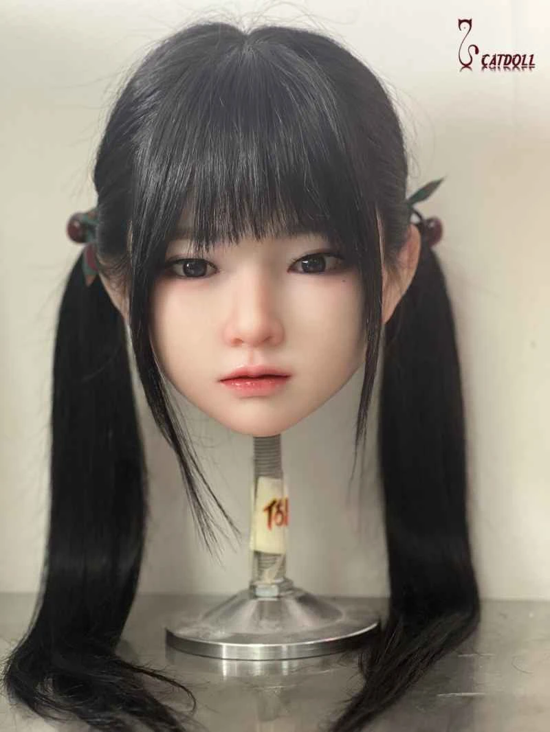
CATDOLL Kara Hard Silicone Head
Articles
2026-02-22
CATDOLL 102CM Li (TPE Body with Soft Silicone Head)
Articles
2026-02-22

CATDOLL 135CM Vivian (TPE Body with Hard Silicone Head)
Articles
2026-02-22