Read next
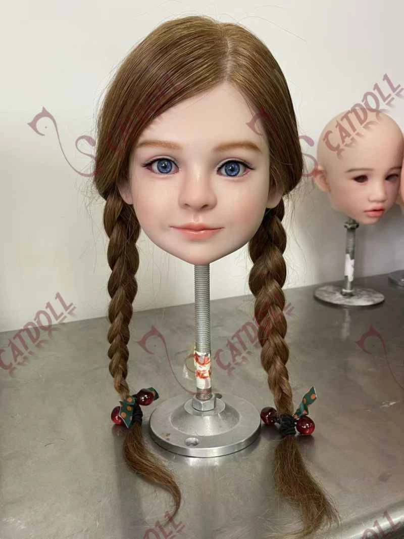
CATDOLL Beth TPE Head
This head is made of TPE material. You can choose the skin tone, eye color, and wig style. It is available with a movab...
Articles
2026-02-22
CATDOLL Rosie Hybrid Silicone Head
Articles
2026-02-22
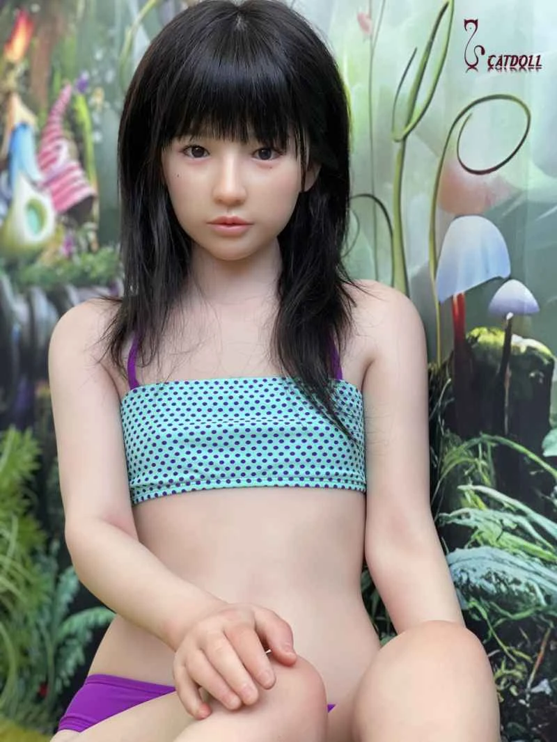
CATDOLL 148CM Qing Silicone Doll
Articles
2026-02-22
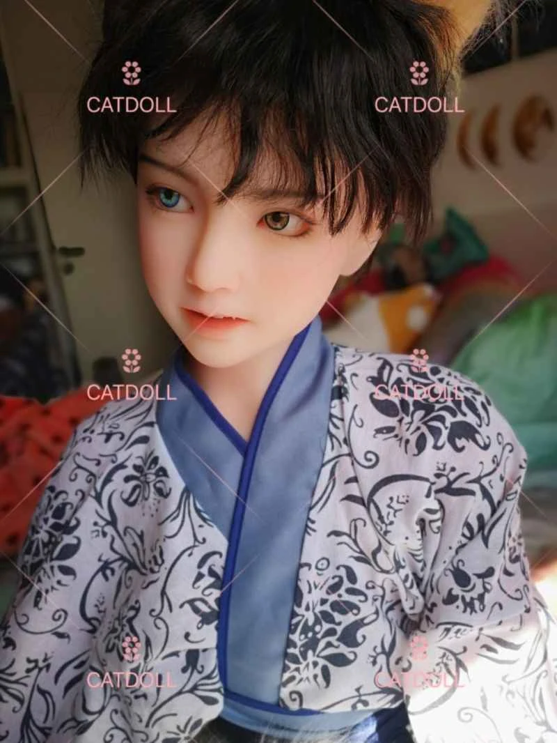
CATDOLL 133CM Ya Shota Doll (Customer Photos)
Articles
2026-02-22