Read next
CATDOLL Yuki Hard Silicone Head
The head made from hard silicone does not have a usable oral cavity. You can choose the skin tone, eye color, and wig, ...
Articles
2026-02-22
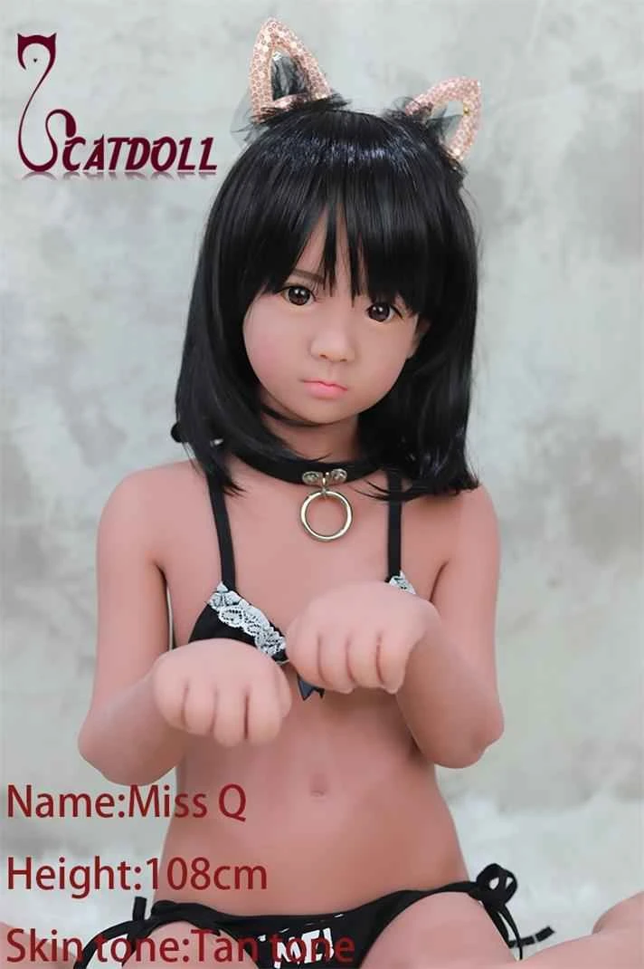
CATDOLL Q 108cm Tan Tone
Articles
2026-02-22
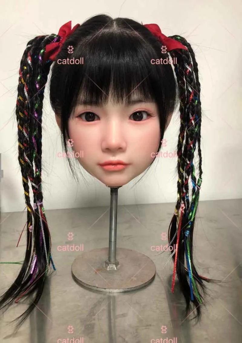
CATDOLL Yuki Hard Silicone Head
Articles
2026-02-22
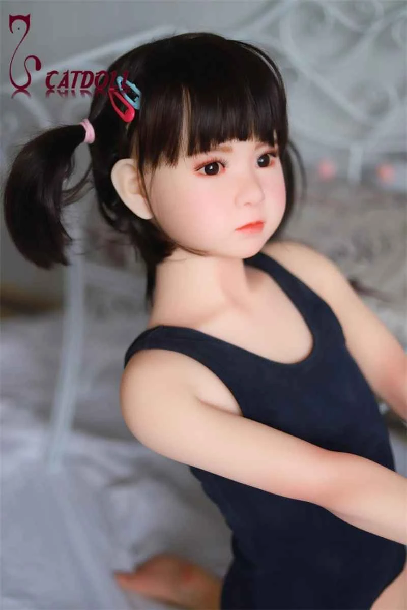
CATDOLL 115CM Kiki TPE
Articles
2026-02-22