Read next
CATDOLL 123CM Tina (TPE Body with Hard Silicone Head)
Height: 123cm Weight: 23kg Shoulder Width: 32cm Bust/Waist/Hip: 61/54/70cm Oral Depth: 3-5cm Vaginal Depth: 3-15cm Anal...
Articles
2026-02-22
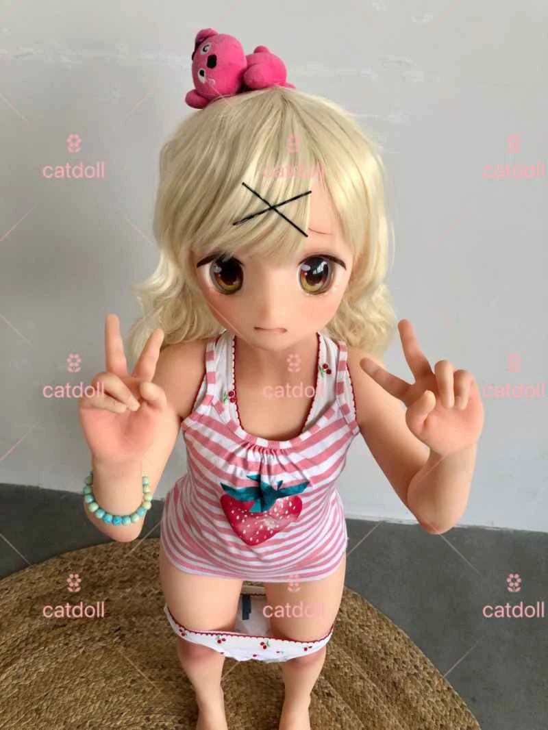
CATDOLL 102CM B04 TPE Doll with Anime Head
Articles
2026-02-22

CATDOLL 135CM Ya
Articles
2026-02-22
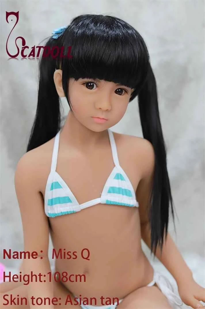
CATDOLL Q 108cm Asian tone – Petite TPE Body with Realistic Features
Articles
2026-02-22