Read next
CATDOLL 128CM Yuki
Height: 128cm Weight: 19kg Shoulder Width: 30cm Bust/Waist/Hip: 57/52/63cm Oral Depth: 3-5cm Vaginal Depth: 3-15cm Anal...
Articles
2026-02-22

CATDOLL 123CM Sasha TPE
Articles
2026-02-22

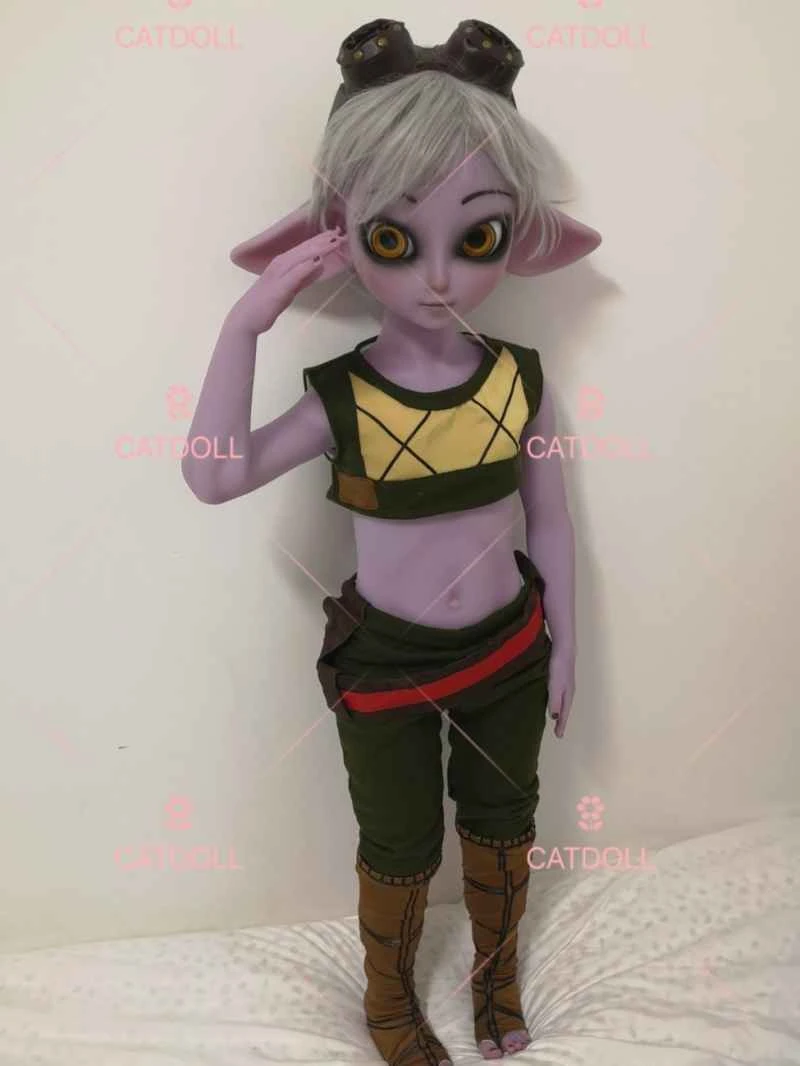
CATDOLL CATDOLL 115CM Darina Silicone Doll
Articles
2026-02-22
CATDOLL CATDOLL 115CM Purple Silicone Doll
Articles
2026-02-22