Read next
CATDOLL 108CM Coco (TPE Body with Hard Silicone Head)
Height: 108cm Weight: 14.5kg Shoulder Width: 26cm Bust/Waist/Hip: 51/47/59cm Oral Depth: 3-5cm Vaginal Depth: 3-13cm An...
Articles
2026-02-22
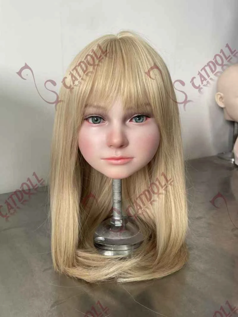
CATDOLL Diana Soft Silicone Head
Articles
2026-02-22

Discussion on the Integration and Upgrading of DCS Control Systems
Articles
2026-02-22

CATDOLL Dodo 109CM TPE
Articles
2026-02-22