Read next
Application and Development Trends of Machine Vision in China's Printing Industry
Machine vision has a 15-year history of development. As an application system, its functional characteristics have gradu...
Articles
2026-02-22
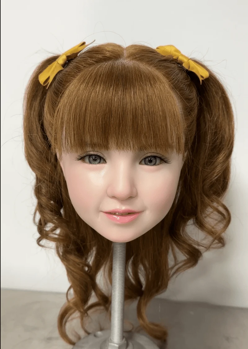
CATDOLL Oksana Hard Silicone Head
Articles
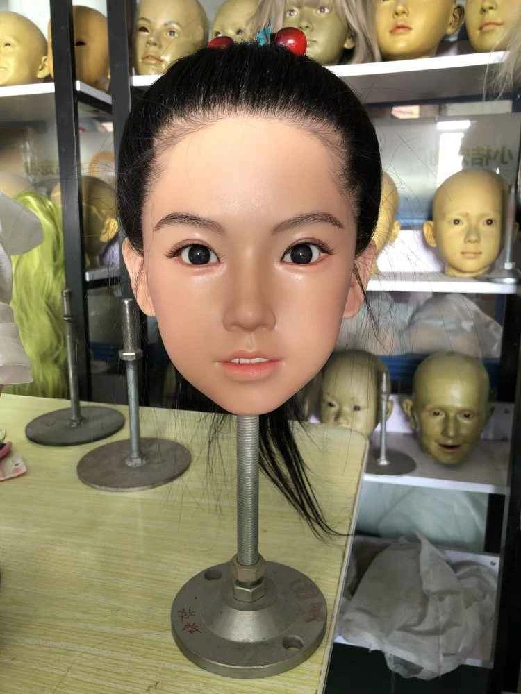
2026-02-22
CATDOLL Vivian Hard Silicone Head
Articles
2026-02-22

CATDOLL 139CM Lucy Silicone Doll
Articles
2026-02-22