Read next
CATDOLL 123CM LuisaTPE
Height: 123cm Weight: 23kg Shoulder Width: 32cm Bust/Waist/Hip: 61/54/70cm Oral Depth: 3-5cm Vaginal Depth: 3-15cm Anal...
Articles
2026-02-22
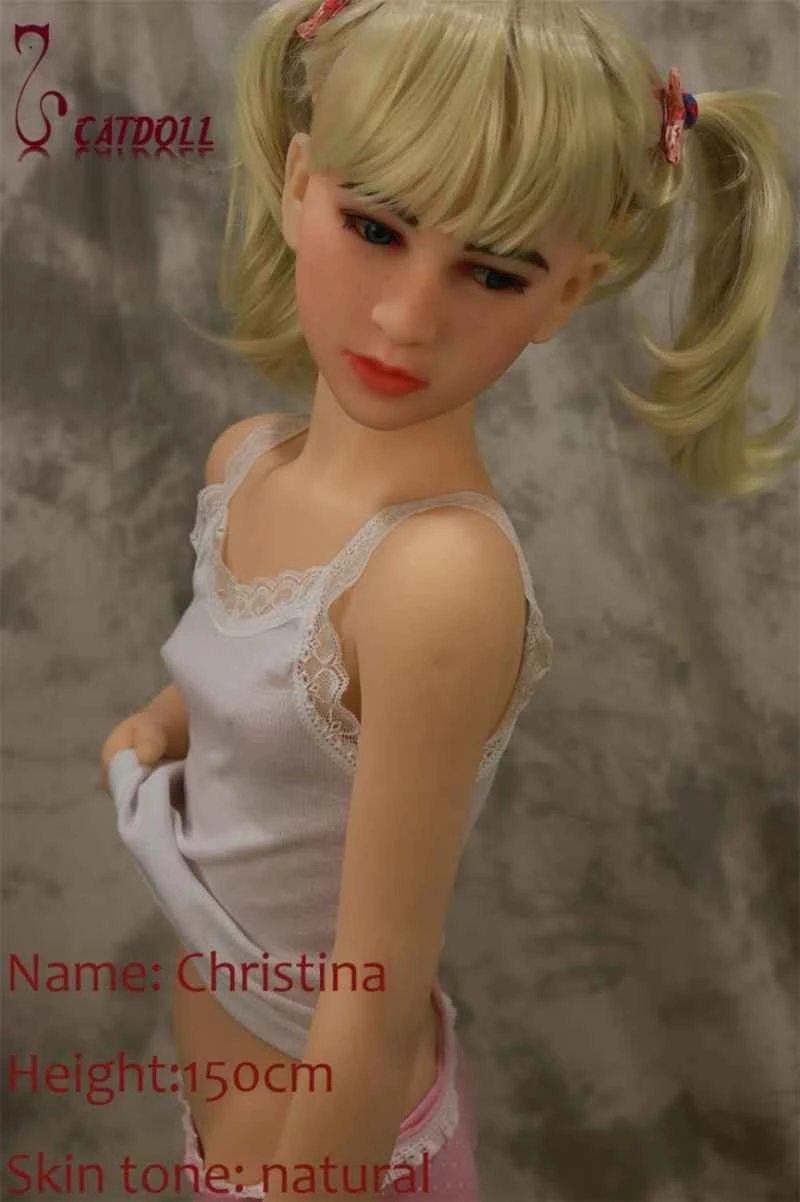
CATDOLL 146CM Christina TPE
Articles
2026-02-22
CATDOLL 136CM Vivian
Articles
2026-02-22

CATDOLL 146CM B-CUP Ya (TPE Body with Hard Silicone Head) Customer Photos
Articles
2026-02-22