Read next
CATDOLL 108CM Dodo – Natural Tone
Height: 108cm Weight: 14.5kg Shoulder Width: 26cm Bust/Waist/Hip: 51/47/59cm Oral Depth: 3-5cm Vaginal Depth: 3-13cm An...
Articles
2026-02-22
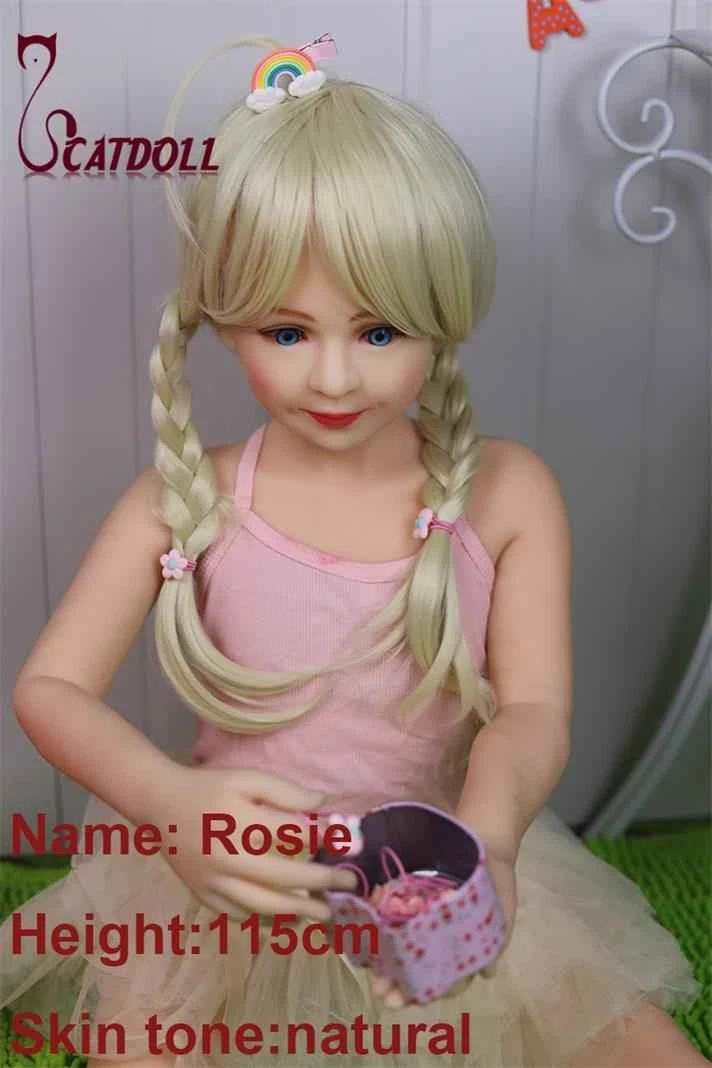
CATDOLL 115CM Rosie TPE
Articles
2026-02-22
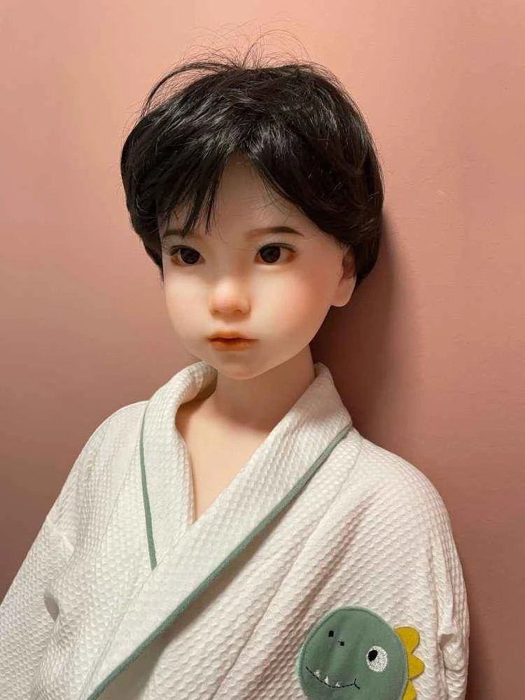
CATDOLL CATDOLL 115CM Shota Doll Nanako (Customer Photos)
Articles
2026-02-22
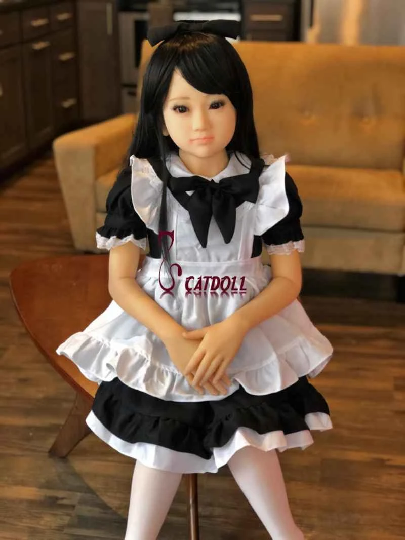
CATDOLL CATDOLL 115CM Saki TPE
Articles
2026-02-22