Read next
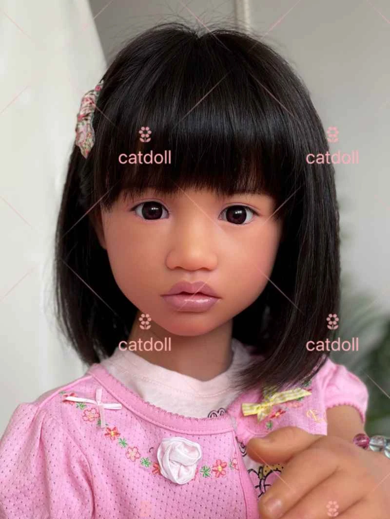
CATDOLL 138CM Tami Silicone Doll
Height: 138 Silicone Weight: 24kg Shoulder Width: 31cm Bust/Waist/Hip: 65/62/78cm Oral Depth: N/A Vaginal Depth: 3-15cm...
Articles
2026-02-22
CATDOLL 108CM Sabrina Full Silicone Doll
Articles
2026-02-22

CATDOLL 101cm TPE Doll with Anime A-01-Type Head
Articles
2026-02-22
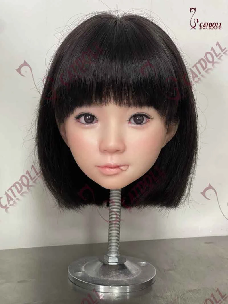
CATDOLL Himari Hybrid Silicone Head
Articles
2026-02-22