Read next
CATDOLL 126CM Sasha (Customer Photos)
Height: 126cm Weight: 23kg Shoulder Width: 32cm Bust/Waist/Hip: 61/58/66cm Oral Depth: 3-5cm Vaginal Depth: 3-15cm Anal...
Articles
2026-02-22
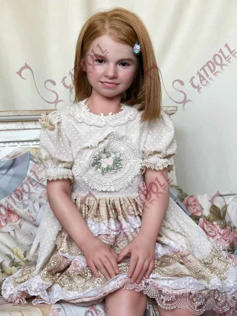
CATDOLL 131CM Amber Silicone Doll
Articles
2026-02-22
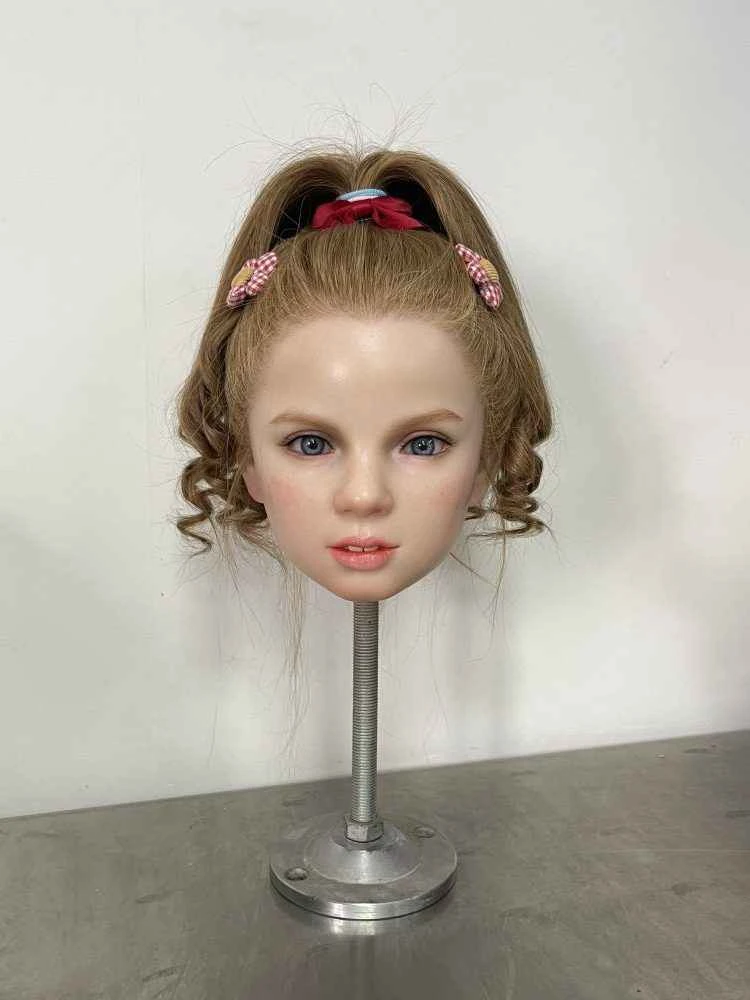
CATDOLL Katya Hard Silicone Head
Articles
2026-02-22
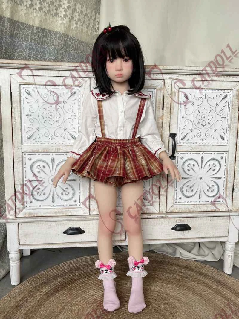
CATDOLL Dodo 109CM TPE
Articles
2026-02-22