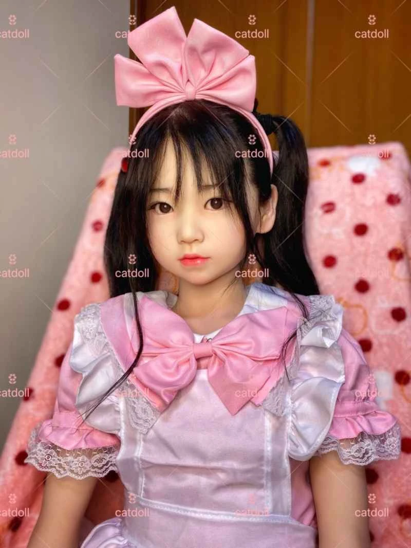
Design of a wireless PC interface card based on the FF protocol
2026-04-06 04:46:35··#1
Abstract: This paper proposes a hardware and software design scheme for a wireless PC interface card based on the FF protocol, taking into account the communication characteristics and requirements of Foundation Fieldbus (FFieldbus). The design effectively solves the local network communication problem in production facilities or industrial sites with moving objects where control nodes are widely distributed and laying communication lines is difficult. Keywords: Foundation Fieldbus; PCI; PC interface card; wireless transceiver chip The design of wireless PC-interface for foundation fieldbus Abstract: This article proposes a software and hardware design scheme for wireless PC-interface based on PCI and nRF401. The PC-interface designed according to this scheme solves satisfactorily the communication problem of the local work located in industrial fields where the controlling points are widely distributed and the lines of communication are difficult to be laid or where mobile devices are used Keywords: foundation fieldbus; PCI bus; PC-interface; wireless transceiver chip 0 Introduction Foundation Fieldbus (FF) is a fieldbus protocol designed by the Fieldbus Foundation to meet the functional, environmental and technical needs of automation systems, especially process automation systems. As a fully digital signal fieldbus protocol, it has gained widespread support internationally [1]. Foundation Fieldbus supports a variety of transmission media, including twisted pair, cable, optical fiber and wireless media. Currently, the first two are more widely used. However, for production facilities with widely distributed control nodes and difficult-to-lay communication lines, or industrial sites with moving objects, wireless data communication must be considered [2, 3]. Therefore, developing wireless communication products based on the FF protocol has significant practical implications. 1 Hardware Design of Wireless PC Interface Card Based on FF Protocol The basic function of the wireless PC interface card based on the FF fieldbus protocol is to be able to communicate autonomously with wireless communication devices conforming to the FF protocol. The overall structure block diagram of the wireless PC interface card is shown in Figure 1. Its hardware circuit includes four parts: the communication interface between the CPU and the PC host CPU, the hardware interface between the CPU and the communication controller, the interface between the communication controller and the data buffer memory, and the interface between the communication controller and the wireless transceiver unit. The dual-port RAM uses the CY7C09449PV-AV chip; the CPU is the Intel80188 CPU, which is most commonly used in embedded control; the communication controller is the FB3050 from SMAR; and the wireless transceiver unit consists of a single-chip wireless transceiver chip nRF401 and its peripheral circuits. The CY7C09449PV-AC can employ bus arbitration and wait mechanisms, allowing both CPUs to share SRAM at the instruction level, exchange information via interrupts, and synchronize via status signals. Communication handshakes and rapid data transfer are performed using status registers and interrupts. 1.1 Interface Card CPU-PC Interface: With the development of computer technology, PC buses are constantly evolving. Considering the trend towards 32/64-bit width and maximum transfer rate (industry standard structure) buses, and taking into account current needs and future development, the PCI bus is chosen as the host bus. The hardware interface chip is a dual-port PCI bus RAM from Cypress Semiconductor. CY7C09449PV-AC is a dual-port RAM interface chip with complete functions and low price that is suitable for PCI2.2 bus specification. One port is a PCI interface, which is suitable for communication with PC. The other port is a local interface, which is suitable for communication with various local CPUs. Its bus communication clock rate can reach 50MHz. Both ports can independently read/write static memory SRAM. Its main features are as follows: ① Fully compatible with PCI specification version 2.2; ② 128 k bidirectional static SRAM; ③ Can be used as a master/slave device for data transmission, supports PCI burst mode operation and DMA operation; ④ Has I2O (Intelligent Input/Output) function. When the I2O unit is working, it contains 4 groups of 32-bit FIFO (FirstIn First Out), interrupt register and part of SRAM. The remaining SRAM is used for general storage purposes; ⑤ Supports 3V and 5V voltage operation; ⑥ The chip can be initialized through the I2O bus and the setting parameters are stored in non-volatile NVRAM; ⑦ 160-pin flat square plastic package [4]. The CY7C09449PV-AC can employ bus arbitration and wait mechanisms, allowing both CPUs to share SRAM at the instruction level, exchange information via interrupts, and synchronize through status signals. Communication handshakes and rapid data transfer are performed using status registers and interrupts. 1.2 Interface Card CPU and Communication Controller FB3050 Interface: The FB3050 is a third-generation Foundation Fieldbus Communication Controller chip from SMAR Corporation. This chip conforms to the field physical layer standard specified in ISASP50-2-1992, PART2. The functional block diagram of the FB3050 chip is shown in Figure 2. As can be seen from the figure, the FB3050 is connected to the CPU via a 3-bus interface. The right side shows the memory bus output by the FB3050; both the CPU and the FB3050 can access the memory connected to this bus. The lower part shows the FB3050's connection to the fieldbus network via a media access unit, and the middle part shows the internal functional blocks of the FB3050. The main functions of FB3050 are to drive and receive signals on the bus, convert serial data to parallel data, encode and decode serial data, pack and unpack information frames, generate and verify frame check sequences, etc. [5]. The external signals of FB3050 can be mainly divided into the following four groups: ① Clock and timing function signals. Three inputs are used for the system clock of FB3050, the data transmission rate clock and the system synchronization edge of FB3050. A 125kHz output signal is used for user lines. ② CPU interface signals. The CPU interface signal line is used to connect the interface card microprocessor, including 16 address lines and 8 data lines. It can be connected in the data/address multiplexing mode or directly. When connected in the data/address multiplexing mode, the lower 8 address lines PI-AD-DR [7:0] are connected to signal ground, including two chip select lines, two read/write control lines, and interrupt request output lines; in addition, it includes a PO-READY line, which can be connected to the WAIT line of the microprocessor, so that the DMA of FB3050 and the CPU can share the local memory bus of FB3050. ③ Memory Bus Signals. This set of signals is a memory bus generated by the FB3050 after transforming the CPU's address bus. The transformed memory bus adds 8 extended memory address lines. Combined with the segment address register added internally by the FB3050, the addressing range of the memory bus greatly exceeds the original CPU's 64KB capacity. It also outputs 6 programmable chip select signals. Therefore, this memory bus and the connected memory are shared by the CPU and the FB3050. ④ Fieldbus Interface Signals. The FB3050 has 8 fieldbus interface lines: one data reception signal line PI-PHPDU, receiving bus signals from the media access unit (the received data signal format conforms to the Manchester encoding rules); one data transmission signal line PO-PHPDU, transmitting data to the media access unit; one control line PO-TACT, controlling the operating status of the bus transmitter; and 5 status signal lines used to indicate the FB3050's transmission and reception status. Because the FB3050's interface design fully considers interfacing with Intel CPUs, the interface between the FB3050 and the Intel 80188 is very simple. The Intel 80188's address and data buses can be directly connected to the FB3050's address and data buses. Any one of the four chip select lines MCS0 to MCS3 can be used as the FB3050's memory chip select line. Any one of the seven I/O chip select lines PCS0 to PCS6 can be used as the FB3050's internal memory chip select line. The FB3050 requires 38 I/O port addresses, while each I/O chip select line of the Intel 80188 can provide 128 I/O port addresses, thus fully meeting the requirements. The FB3050's interrupt output is active low, while the Intel 80188 CPU's interrupt input lines require a high level or rising edge signal; therefore, an inverter is needed. The FB3050's READY output line can be directly connected to the Intel 80188's AREADY pin, allowing the FB3050's DMA and CPU to share the FB3050's local memory bus. The Intel 80188's clock output signal can be directly used as the FB3050's system clock input. 1.3 FB3050 Interface with Wireless Transceiver Unit The basic function of the wireless transceiver unit of the wireless PC interface card is to send and receive wireless signals conforming to the FF specification; it is crucial for normal communication using FF signals. Its main component is the single-chip wireless transceiver chip nRF401. The nRF401 is a newly launched single-chip wireless transceiver chip from Nordic Corporation, operating in the ISM band (433MHz). It is currently the most highly integrated wireless data transmission product, packaged in a 20-pin dual in-line package. The nRF401 internally includes high-frequency receiving/transmitting, PLL combining, FSK modulation/demodulation, and dual-frequency switching units. The chip has the following features: FSK modulation mode, direct data input and output, strong anti-interference ability, especially suitable for industrial occasions; adopts DSS+PLL frequency synthesis technology, with excellent frequency stability; high sensitivity, reaching -105dBm; no Manchester encoding required; working rate up to 20kb/s; maximum transmit power up to +10dBm; the maximum operating distance in open areas up to 1000m; operates in the ISM band 433MHz and dual-channel frequencies 433.92MHz/433.34MHz, and does not require a license[6]. The schematic diagram of the wireless transceiver unit and the interface circuit of FB3050 implemented using nRF401 is shown in Figure 3. Among them, the antenna design of the wireless transceiver unit adopts a loop differential antenna. The clock input of nRF401 must be synchronized with the CPU and FB3050, so nRF401 must share a clock source with the CPU and FB3050. The data output (DOUT)/input (DIN) of the nRF401 chip is connected to the receive input (PI-PHPDU) and transmit output (PO-PHPDU) signal lines of the FB3050; it is connected to the FB3050's data transmit enable signal pin PO-TACT. When PO-TACT outputs a high level, it is in transmit mode; otherwise, it is in receive mode. CS is the frequency selection pin, connected to a PCB jumper, and the frequency used is selected by high or low levels; PWR-UP is the power-saving mode selection signal pin, also connected to a PCB jumper. A high level indicates operating mode, and a low level indicates standby mode. 2. Software Design The software of the wireless PC interface card is designed using an embedded design method. Its basic working process is as follows: When there is an external signal, the wireless transceiver unit first receives the signal and sends it to the communication controller FB3050. The communication controller receives the signal and sends it to the receive buffer on the interface card, and then the CPU on the interface card responds. Commands and data that can be processed are processed immediately, and the rest are transmitted to the host computer for processing through the PCI dual-port RAM interface. Conversely, when the host computer needs to send information to the FF-based wireless network, the signal first passes through the PCI dual-port RAM, then through the interface card CPU to the communication card's transmit buffer, and finally the communication controller sends the contents of the transmit buffer to the wireless network via the wireless transceiver unit. The FF communication controller FB3050 uses DMA for both receiving and sending messages to the wireless transceiver unit. The FB3050 has a direct memory access table, which greatly simplifies receiving and sending operations. Using this DMA table, the FB3050 can directly store received information into memory or send information from memory without CPU intervention. During reception, the user only needs to specify the memory area of the receive buffer, and the FB3050 automatically stores the information into the buffer sequentially. The buffer is a circular contiguous space, so when data (information) reaches the end of the buffer, the FB3050 will return to the buffer's start pointer and continue writing the next received byte. The buffer requires 4 KB or more of space. When sending data, the user only needs to specify the length of the start pointer. The FB3050 sends this information to the wireless transceiver unit upon receiving the send command, and then the information is transmitted to the FF wireless network via the wireless transceiver unit. 3. Conclusion The FF protocol-based wireless PC interface card designed according to the above scheme effectively solves the local network communication problem in production equipment or industrial sites with moving objects where control nodes are widely distributed and laying communication lines is difficult. It basically meets the requirements of industrial control in terms of anti-interference capability, real-time performance, and reliability. With the maturity of the technology and its wider application, the development trend of industrial control systems will inevitably shift from wired networks to wired-wireless hybrid networks. The development of FF-based wireless network product software and hardware will promote the widespread application of industrial control networks and generate significant social and economic benefits. References [1] Feng Dongqin, Shi Yiming. Foundation Fieldbus (FF) Technology Lecture (Lecture 1): Development and Characteristics of Foundation Fieldbus (FF) [J]. Shanghai: Automation Instrumentation, 2001, 22(6): 52-54. [2] Shen Gang, He Xing. Design and Implementation of Wireless Gateway for Industrial Control Network [J]. Lanzhou: Chemical Automation and Instrumentation, 2001, 28(6): 37-41. [3] Cavalieri S, Panno DAA Novel Solution to InterconnectFielBus Systems Using IEEE Wireless LAN Technology [J]. Computer Standards & Interfaces. 1998, (20): 9-23. [4] Li Guishan, Wei Dehu. PCI Local Bus Developer's Guide [M]. Xi'an: Xi'an University of Electronic Science and Technology Press, 1997. [5] Cai Jianxin, Yan Huawen. Principle and application of fieldbus communication controller FB3050 [J]. Xi'an: Foreign Electronic Components, 2000, (6): 5-11. [6] Zhang Ming, Liu Yinfeng. Design of PC wireless transceiver module based on nRF401 [J]. Beijing: Electronic Technology Application, 2002, 28(4): 76-78. Industrial Instrumentation and Automation Devices