Read next
CATDOLL 128CM Yuki
Height: 128cm Weight: 19kg Shoulder Width: 30cm Bust/Waist/Hip: 57/52/63cm Oral Depth: 3-5cm Vaginal Depth: 3-15cm Anal...
Articles
2026-02-22
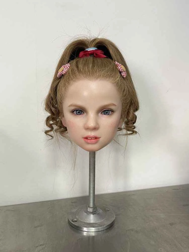
CATDOLL Katya Hard Silicone Head
Articles
2026-02-22


Green lighting and intelligent lighting energy-saving control system
Articles
2026-02-22