Read next
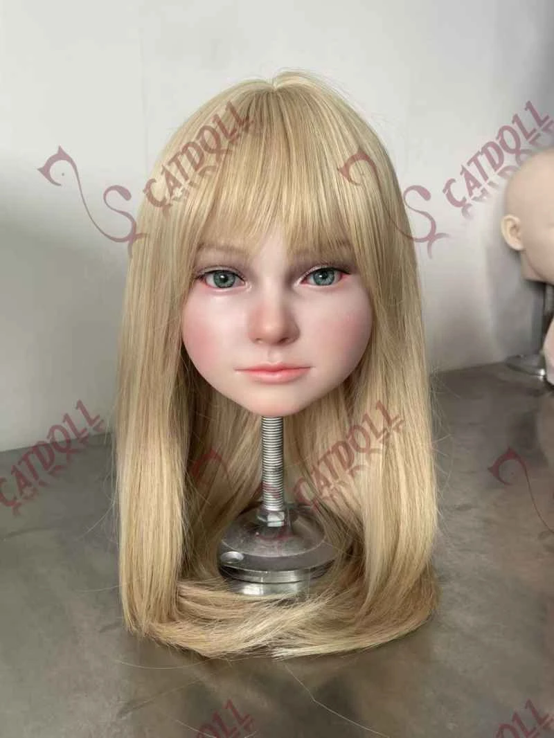
CATDOLL Ava Soft Silicone Head
You can choose the skin tone, eye color, and wig, or upgrade to implanted hair. Soft silicone heads come with a functio...
Articles
2026-02-22

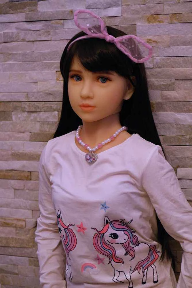
CATDOLL 138CM Ya TPE (Customer Photos)
Articles
2026-02-22
CATDOLL Diana Soft Silicone Head
Articles
2026-02-22
CATDOLL 146CM Sasha TPE (Customer Photos)
Articles
2026-02-22