Read next
CATDOLL 60CM Sasha Silicone (Elf Ear)
Height: 60cm Silicone Weight: 2.7kg Shoulder Width: 14cm Bust/Waist/Hip: 27/24/31cm Oral Depth: N/A Vaginal Depth: 3-8c...
Articles
2026-02-22
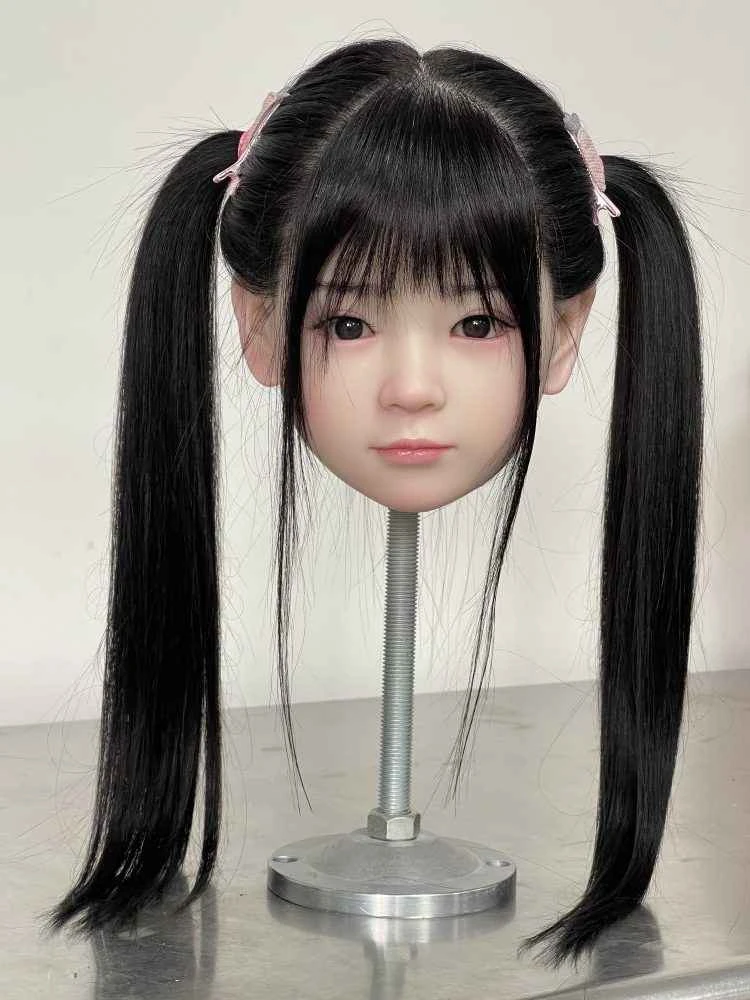
CATDOLL Cici Hard Silicone Head
Articles
2026-02-22

CATDOLL 133CM Kiki Shota Doll
Articles
2026-02-22
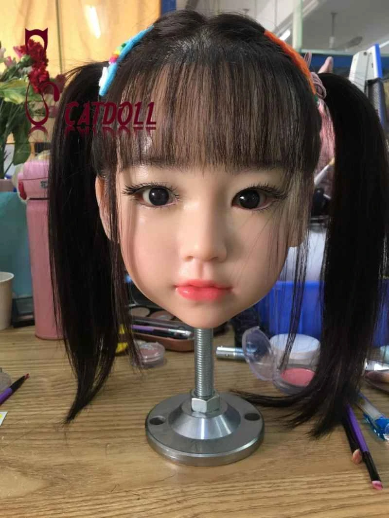
CATDOLL Nanako Hard Silicone Head
Articles
2026-02-22