Read next
CATDOLL CATDOLL 115CM Saki TPE
Height: 115cm Weight: 19.5kg Shoulder Width: 29cm Bust/Waist/Hip: 57/53/64cm Oral Depth: 3-5cm Vaginal Depth: 3-15cm An...
Articles
2026-02-22

Measures for the sustainable development of concrete construction machinery
Articles
2026-02-22
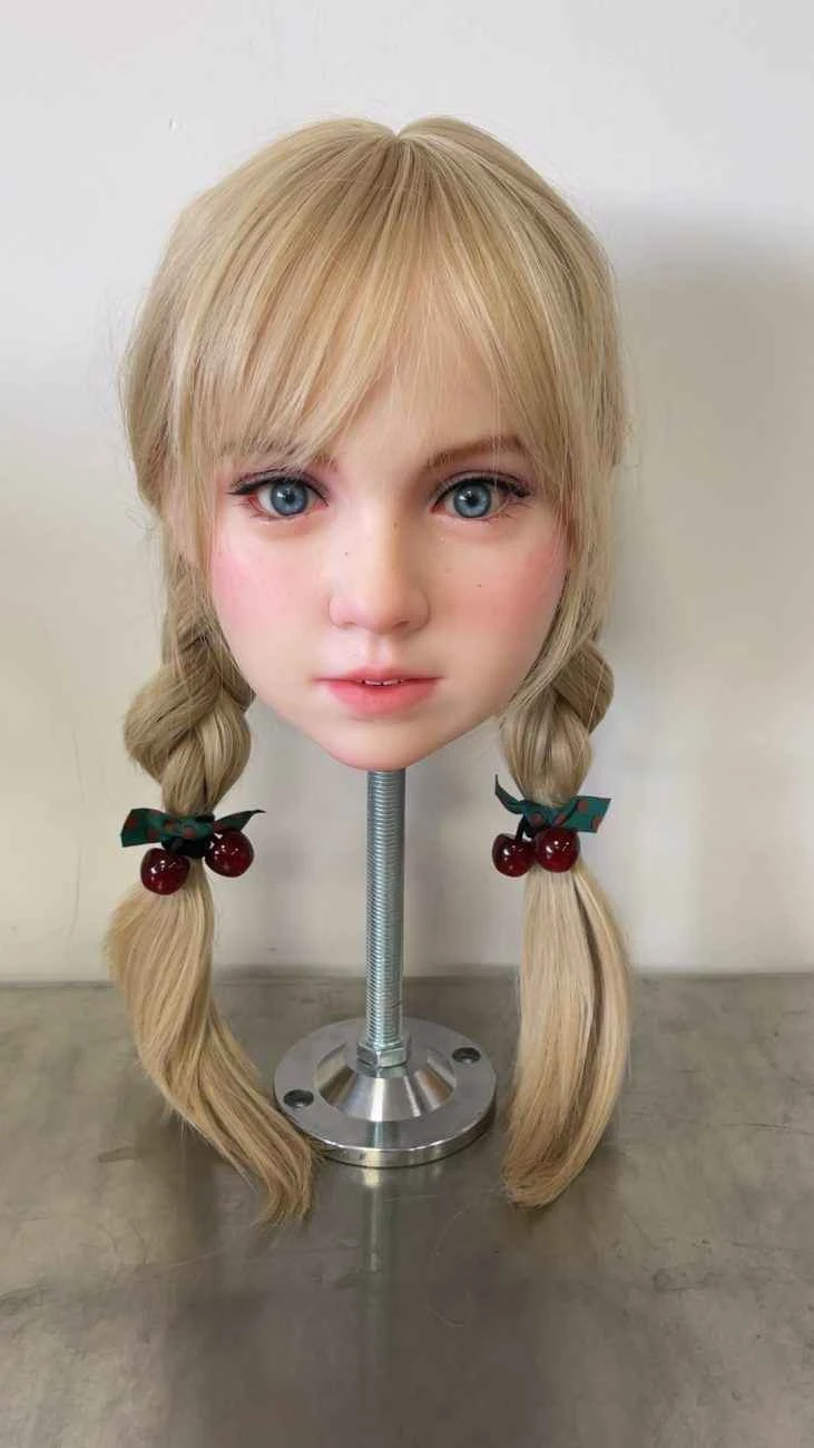
CATDOLL Sasha Soft Silicone Head
Articles
2026-02-22
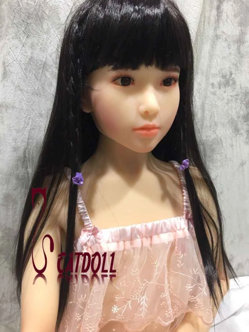
CATDOLL 136CM Tami
Articles
2026-02-22