Read next
CATDOLL 148CM Sana Silicone Doll
Height: 148 Silicone Weight: 33kg Shoulder Width: 34cm Bust/Waist/Hip: 70/58/82cm Oral Depth: N/A Vaginal Depth: 3-15cm...
Articles
2026-02-22
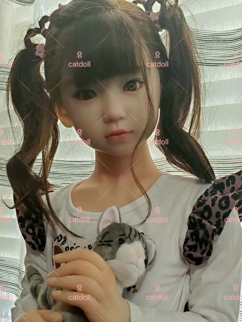
CATDOLL CATDOLL 115CM Nanako (TPE Body with Hard Silicone Head) Customer Photos
Articles
2026-02-22
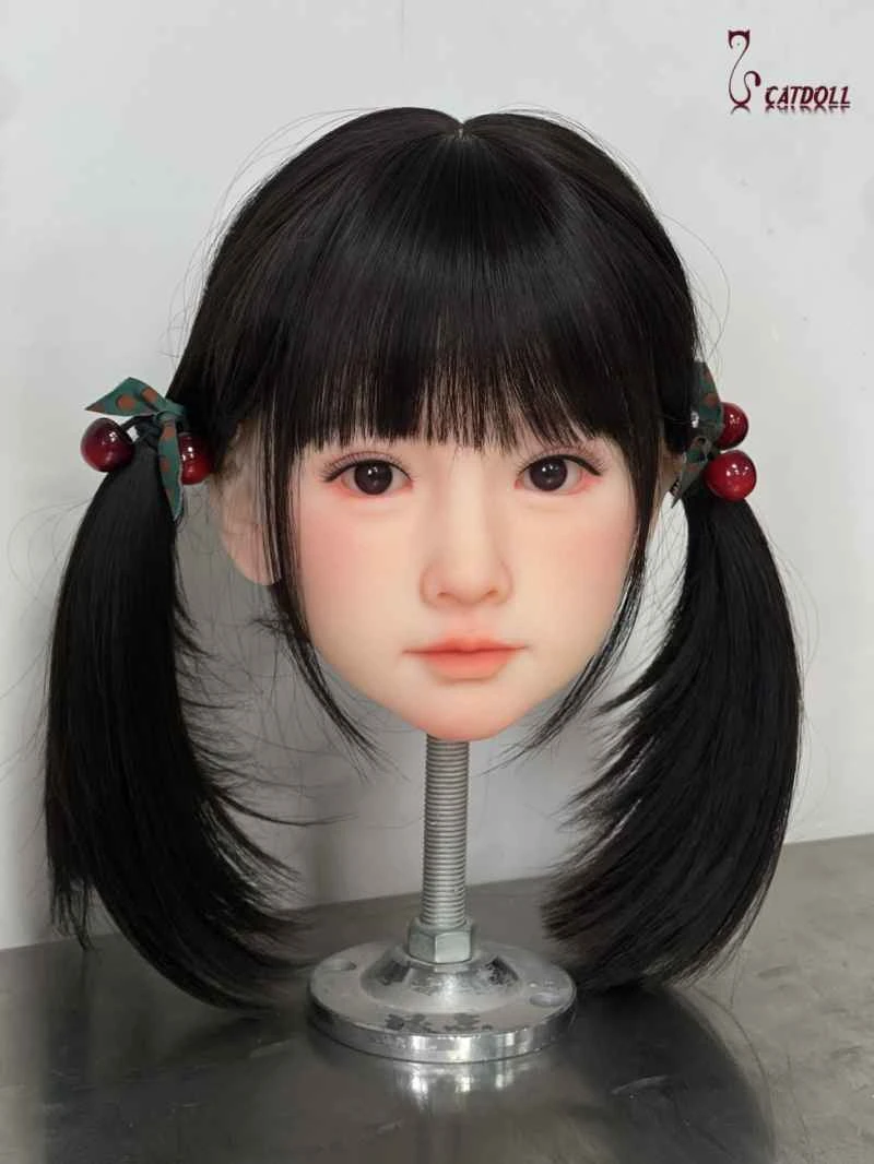
CATDOLL Airi TPE Head
Articles
2026-02-22
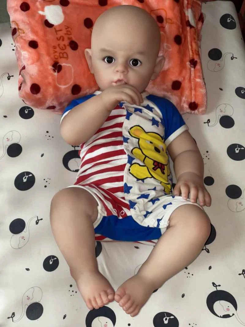
CATDOLL 66cm Baby Boy Silicone Doll – Lifelike Newborn Style
Articles
2026-02-22