Read next
CATDOLL CATDOLL 115CM Nanako (TPE Body with Hard Silicone Head)
Height: 115cm Weight: 19.5kg Shoulder Width: 29cm Bust/Waist/Hip: 57/53/64cm Oral Depth: 3-5cm Vaginal Depth: 3-15cm An...
Articles
2026-02-22
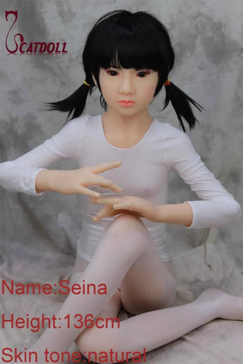
CATDOLL 136CM Seina
Articles
2026-02-22

CATDOLL 128CM Dolly Silicone Doll
Articles
2026-02-22

CATDOLL 130CM Sasha
Articles
2026-02-22