Share this

Design of low-voltage high-current switching power supply

2026-04-06 04:31:11 · · #1
Abstract : This article introduces the principle and design method of active clamped synchronous rectification forward converter. With the design equation and experimental prototype presented, it can be proved that the converter mentioned above represents the best topology for low voltage & high current SMPS. Keywords : active clamped forward converter, synchronous rectification [b]1 Introduction[/b] To achieve higher speed and better performance with lower power consumption, the power supply voltage is required to be increasingly lower, and the transient performance indicators are increasingly higher, thus placing increasingly higher demands on switching power supplies. Existing circuit topologies and rectification methods can no longer meet current requirements. To adapt to the needs of IC chip development, people have begun to study new circuit topologies. Because the output voltage is very low, synchronous rectification naturally becomes the inevitable choice for this type of low-voltage, high-current power supply. Considering the complexity and reliability of the product, self-driven synchronous rectification is generally chosen. There are roughly three types of topologies that can be well integrated with self-driven synchronous rectification circuits: active clamped forward converter; complementary control half-bridge converter; and two-stage converter. Compared to two-stage converters, active clamp converters and complementary control half-bridge converters use fewer components and are more attractive. These two converter topologies easily implement soft switching and can operate at higher frequencies; the transformer cores can be bidirectionally magnetized, resulting in high core utilization. For a primary rectified power supply output of -48V (36~72V), when the input voltage varies over a large range (36~72V), the driving voltage variation range obtained by the secondary side of the complementary control half-bridge circuit is too large to drive MOSFETs. Therefore, the active clamp self-driven synchronous rectified forward converter is the inevitable circuit topology for low-voltage, high-current switching power supplies. [b]2 Topology Analysis of Active Clamp Synchronous Rectified Forward Converter[/b] The circuit topology of the active clamp synchronous rectified forward converter is shown in Figure 1. The main parameter waveforms of the DC-DC active clamp ZVS-PWM forward converter during steady-state operation within one switching cycle are shown in Figure 2. One switching cycle can be roughly divided into four operating modes, namely: 1) to 3. Circuit Parameter Design and Calculation Formulas The main circuit topology is shown in Figure 1. Its clamping capacitor voltage is: Vc1 = DVin / (1-D). The clamping capacitor's withstand voltage must be greater than this value. Sufficient capacitance is sufficient to ensure normal circuit operation. In this design, a 47μF clamping capacitor was selected. The UC3823N control chip is used to implement PWM control. The control chip detects the switching current and adds a ramp signal (generated from pin 14 of the PWM output signal) to the chip's current terminal (pin 7). The voltage signal is divided by a sampling resistor and compensated by an error amplifier to generate an output signal (pin 3). This signal is compared with the signal at pin 7 to generate the output duty cycle signal PWM. Then, a pulse transformer isolates and a primary-side driver UC1707 generates two complementary pulse drive converters with adjustable dead time, controlling the main transistor S1 and clamping transistor S2. Appropriate parameter design, especially the selection of the voltage compensator and ramp compensation, will ensure stable and reliable system operation. Based on theoretical analysis and practice, when designing an active clamped synchronous rectifier forward converter, it is necessary to calculate various parameters. In the process of practice, a set of formulas for designing converters has been summarized. These formulas are given below for reference. In addition, it should be noted that the values ​​calculated by the formulas should also leave an appropriate margin to ensure the reliability of the power supply. (1) Number of primary turns of transformer N1 N1=U·D·104/f·△Bm·Ac Where U is the input voltage; D is the duty cycle; f is the switching frequency; △Bm is the magnetic induction increment; Ac is the effective area of ​​the magnetic core. (2) Number of secondary turns of transformer N2 N2=N1·Vo/D Where Vo is the output voltage. (3) Determination of primary inductance Lprim The primary inductance Lprim is determined by the following formula Lprim=uo·ua·N12·Ae/le Where uo is the vacuum permeability; ua is the amplitude permeability; N1 is the number of primary winding turns; Ae is the effective cross-sectional area of ​​the magnetic core; le is the effective magnetic path length. (4) Output voltage Vo = D·Vin·N1/N2 (5) Calculation of output inductance L and capacitance C L = 2.5R/f Take IL (peak) = 1.1Io C = △IL/8f△Vo ESR (max) = △Vo/△IL Where △IL = 0.2Io (6) Parameters of conductor Cross-sectional area and diameter of conductor d Sm = Ii/J di = 1.13Sm1/2 Where Ii is the effective value of current of each winding (A); J is the current density, which is calculated based on copper loss. According to engineering practice, the current density of conductor is selected as 2-4 (A/mm2) when naturally cooled, and 3-5 (A/mm2) when forced cooled. The value is appropriate. When calculating the required conductor diameter, the influence of skin effect should be considered. When the conductor diameter is greater than twice the skin depth, multi-strand conductors should be wound in parallel as much as possible. When n strands of wire are wound in parallel, the diameter din of each strand is calculated using the following formula: din = di / n<sup>1/2</sup>. The skin depth Δ of the copper wire has the following empirical formula: Δ = 66.1 / f<sup>1/2</sup>. After calculating Δ using the above formula, compare it with di. When di is greater than 2Δ, multiple strands of wire should be wound in parallel, and the value of n should be such that din is not greater than 2Δ. 4. Problems and Solutions of Synchronous Rectification Technology The basis of synchronous rectification technology is the application of MOSFETs to replace diode rectifiers. However, MOSFETs, when used as switches, have bidirectional conduction characteristics. This characteristic causes the following problems in the use of converters containing synchronous rectification technology. 4.1 Problems with Parallel Operation of Synchronous Rectification Converters Synchronous rectification technology is generally used in low-voltage, high-current applications. Therefore, multiple converters with synchronous rectification technology are often connected in parallel. When the output voltages of two parallel converters differ, and the difference reaches a certain value, the output current of the converter with the lower output voltage will reverse. The converter with the higher output voltage will then supply current to both the load and the converter with the lower output voltage, thus increasing the load on the converter with the higher output voltage. As a result, the purpose of parallel operation—to increase the load current—is not achieved. Additionally, there is the problem of self-oscillation, which will increase the voltage stress on the MOSFETs and introduce harmonic interference to the converter output. To address this problem, we have designed a voltage adjustment terminal for the power supply, allowing the output voltage to be continuously adjusted within a certain range. If the user needs parallel operation, they only need to precisely adjust the voltage to be consistent. 4.2 Efficiency Issues Under light load conditions, converters using diode rectifiers enter discontinuous current processing mode (DCM). However, for converters using synchronous rectification technology, due to the bidirectional conduction of MOSFETs, the load current continues to flow in reverse through the output inductor, forming a loop current and causing unnecessary losses, thus limiting the converter's ability to achieve high efficiency under light load conditions. Furthermore, efficiency also changes significantly with input voltage variations. These are all due to the converter operating in different modes, resulting in energy flow feedback. These problems are discussed in detail and solutions provided in reference 7. 5 Experimental Results A secondary power supply module was designed using the circuit topology and parameters analyzed above. The prototype parameters are as follows: input voltage 48V (36-72V), output voltage/current 2.1/40A, switching frequency 250KHz, transformer core EC28 ferrite, main switch S1 and clamping transistor S2 IRF640, synchronous rectifier IRL3803S with an on-state resistance Rds of only 6mΩ. At an input voltage of 48V, the full-load efficiency is 85%. After small-batch production and fine-tuning of circuit parameters, the product's performance in all aspects meets the requirements, and mass production has now begun. 6. Conclusion This paper introduces the working principle, circuit parameters, and calculation formulas of an active clamp self-driven synchronous rectifier forward converter. This circuit topology can effectively realize a low-voltage, high-current switching converter. This solution achieves high efficiency and high reliability, while also realizing low-voltage, high-current output, meeting the needs of the IT industry. Therefore, this solution has significant market application value. References (1) Ionel Dan Jitaru, George Cocina. High Efficiency DC-DC Converter, APEC'94 (2) Wojcieh A. Tabisz, Fred C. Lee and Dan Y. Chen, A MOSFET Resonant Synchronous Rectifier for High-frequency DC/DC Converter, PESC, 1990. (3) Liaan YC, Orugant R, Oh T B. Design considerations of power MOSFET for high frequency synchronous rectification. IEEE Trans on Power Electronics, 1995, 10 (3). (4) Teruhiko KOHAMA, Tamotsu NINOMIYA, Masahito SHOYAMA. Abnormal Phenomena Caused by Synchronous Rectirers in Parallel-module DC-DC Converter System. IEEE APEC'1998 Record: 1225-1229. (5) H. Tanaka, T. Ninomiya, YoOkabe, T. Zaitsu. Low Noise Characteristics of a ZVS-PWM Controlled Serie Resonant Converter with Active Clamp and Synchronous Rectification. IEEE APEC'99 Record, Vol.1:146-152, May 1999. (6) Zhang Zhansong, Cai Xuansan. Principles and Design of Switching Power Supplies. Electronic Industry Press, 1999. (7) Qu Chengming, Wang Huizhen. Research on Improving Synchronous Rectification Efficiency in Active Clamp ZVS-PWM Controlled Series Resonant Converters. Power Supply Technology Application, 2002, 10:28-32. (8) Zhang Xingzhu. Multi-output Precision DC Switching Regulated Power Supply System for Satellites. Power Supply World, 2002, 2:22-25. (9) Liu Jun, Yan Yangguang, et al. Research on active clamp forward DC/DC converter with synchronous rectification. Proceedings of the 14th National Conference on Power Supply Technology. Beijing, 2001, 9. (10) Wang Hao, et al. Status and development of low voltage high current synchronous rectification technology. Power Supply Technology Application, 2002, 9: 56-59. (11) Zhao Liangbing. Fundamentals of Modern Power Electronics Technology. Tsinghua University Press, 1995.
Read next

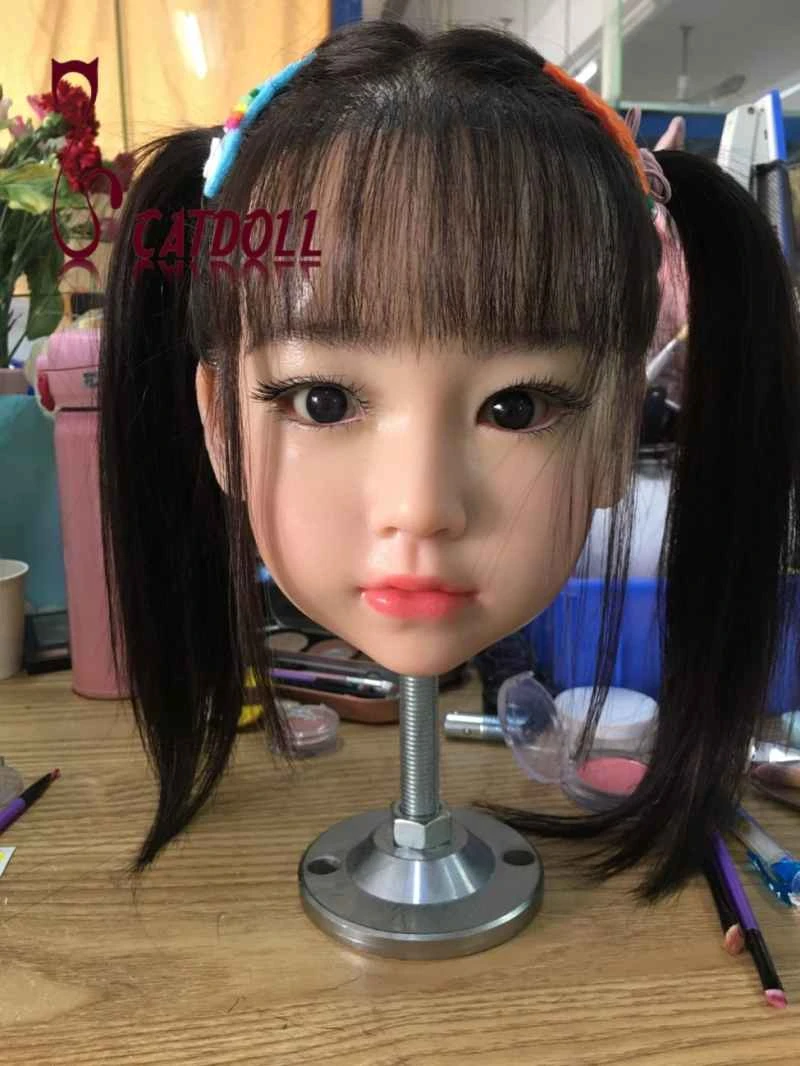
CATDOLL Coco Soft Silicone Head

You can choose the skin tone, eye color, and wig, or upgrade to implanted hair. Soft silicone heads come with a functio...

Articles 2026-02-22