Read next
CATDOLL 108CM Coco
Height: 108cm Weight: 14.5kg Shoulder Width: 26cm Bust/Waist/Hip: 51/47/59cm Oral Depth: 3-5cm Vaginal Depth: 3-13cm An...
Articles
2026-02-22
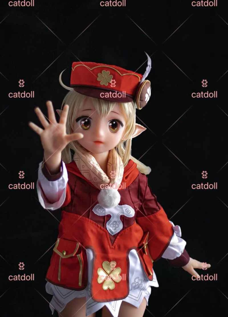
CATDOLL 101cm TPE Doll with Anime A-Type Head – Cute Petite Body
Articles
2026-02-22

CATDOLL 126CM Emelie
Articles
2026-02-22
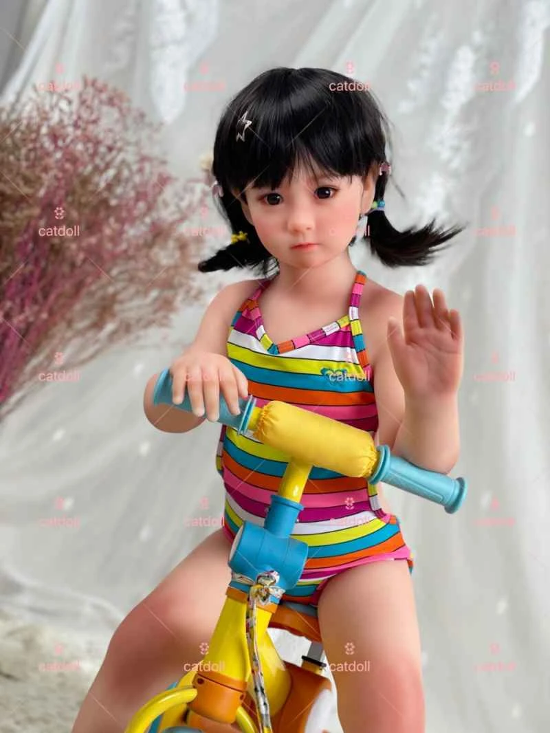
CATDOLL Q 92CM Body with TPE Material
Articles
2026-02-22