Share this

Design of a Sine Wave Output Inverter Power Supply Based on a Microcontroller

2026-04-06 07:31:20 · · #1
Abstract: This paper introduces the design of a sinusoidal output inverter power supply. The design employs a two-stage DC/DC and DC/AC converter, high-frequency transformer isolation, and microcontroller control. Experimental results show reliable performance. Keywords: Inverter power supply; Microcontroller; Sinusoidal pulse width modulation 0 Introduction Low-voltage, low-power inverter power supplies have been widely used in industrial and civilian fields. Especially with the development and utilization of new energy sources, such as the widespread use of solar cells, an inverter system is needed to convert the DC voltage output from solar cells to 220V, 50Hz AC voltage for convenient use. This paper presents the design of a sinusoidal output inverter power supply controlled by a microcontroller. It takes a 12V DC power supply as input and outputs a 220V, 50Hz, 0-150W sinusoidal AC power supply to meet the power supply needs of most common small electrical appliances. The power supply adopts a push-pull boost converter and a full-bridge inverter two-stage converter, with complete isolation between the front and rear stages. In the control circuit, the front-end push-pull boost circuit uses an SG3525 chip for control, sampling the transformer winding voltage for closed-loop feedback; the inverter section uses a single-chip microcomputer digital SPWM control method, sampling the DC bus voltage for voltage feedforward control, and simultaneously sampling the current for feedback control; in terms of protection, it has multiple protection circuits including input over/under voltage protection, output overload/short circuit protection, and overheat protection, enhancing the reliability and safety of the power supply. This power supply can output a 220V±10V sinusoidal AC voltage with a frequency of 50Hz±0.5Hz and a DC component of 1% within an input voltage range of 10.5V to 15V. Main Circuit The main circuit of the inverter power supply uses a two-stage conversion process: push-pull boost and full-bridge inverter, as shown in Figure 1. One end of the input voltage is connected to the center tap of the primary winding of the transformer, and the other end is connected to the midpoint of switching transistors S1 and S2. Controlling S1 and S2 alternately generates a high-frequency AC voltage on the primary side of the transformer. After transformer boosting, rectification, and filtering, approximately 370 V DC voltage is obtained across capacitor C1. The inverter bridge composed of S3 to S6 employs sinusoidal pulse width modulation. The inverter output voltage, after filtering through inductor L and capacitor C2, finally provides a 220 V, 50 Hz sinusoidal AC current to the load. Using a high-frequency transformer for isolation between the front and rear stages improves system safety. The input voltage is 10.5–15 V, and the maximum input current is 15 A. Considering a margin of 10%, the push-pull circuit switches S1 and S2 have a withstand voltage of no less than 30 V and a forward current of no less than 30 A; the IRFZ48N is selected. The design of the boost high-frequency transformer should ensure that, at the lowest input voltage, the rectified secondary voltage is no less than the minimum voltage of 350 V required by the inverter section, while at the highest input voltage, the secondary voltage should not be too high to avoid damaging components. Voltage drop and heat generation on the windings must also be considered. EE-type ferrite cores are selected, with a primary-to-secondary winding ratio of 7 turns:300 turns. For high-frequency transformer design, please refer to the relevant literature. The secondary output rectifier bridge consists of four HER307 capacitors. 68μF, 450V electrolytic capacitors are used for the filter. Based on the output power requirements, the effective output current is 0.6–0.7 A. Considering a certain voltage and current margin, IRF840 capacitors are selected for S3–S6 in the inverter bridge. The inverter section adopts unipolar SPWM control with a switching frequency fs = 16 kHz. Assuming the filter time constant is 16 times the switching period (i.e., the resonant frequency is 1 kHz), the filter inductor and capacitor LC ≈ 2.5 × 10⁻³, which can be selected as L = 5 mH and C = 4.7 μF. The filter inductor L is a toroidal iron powder core with an inner diameter of 20 mm and an outer diameter of 40 mm, wound with two strands of 0.4 mm diameter enameled wire in parallel, with 180 turns. 2. Digital SPWM Control Method The control circuit of this inverter power supply is also divided into two parts. The front-stage push-pull boost circuit is controlled by the dedicated PWM chip SG3525, sampling the transformer winding voltage to achieve voltage closed-loop feedback control. The rear-stage inverter circuit is controlled by the microcontroller PIC16C73, sampling the bus voltage to achieve voltage feedforward control. The front-stage control method is relatively simple; here, we mainly introduce the digital SPWM control method of the rear-stage microcontroller. 2.1 Sinusoidal Pulse Width Modulation (SPWM) Sinusoidal pulse width modulation (SPWM) technology has advantages such as linear voltage regulation and harmonic suppression, and is currently the most widely used pulse width modulation technology. Generally, a triangular wave μc is used as the carrier signal, and a sine wave ug = UgmSin2πfgt is used as the modulation signal. Based on the intersection of μ and μg, a series of pulse signals with pulse widths varying sinusoidally are obtained. The modulation ratio m = Ugm/Ucm and the frequency ratio K = fc/fa = Tg/Tco can then be defined. Sinusoidal pulse width modulation can be divided into unipolar SPWM and bipolar SPWM. Bipolar SPWM uses a symmetrical triangular wave carrier with both positive and negative half-cycles, and the output voltage is an alternating positive and negative square wave sequence without a zero level. Therefore, it can be applied to half-bridge and full-bridge circuits. In practice, the frequency ratio K should be chosen to be odd, so that the output voltage μo has odd function symmetry and half-wave symmetry, and μc has no even-order harmonics. However, the output voltage μc contains a relatively serious n=K-th center harmonic and n=jk±6-th sideband harmonics. Its control signal is two pulse signals with complementary phases. Unipolar SPWM uses a unipolar asymmetrical triangular wave carrier, and the output voltage is also a unipolar square wave. Because the output voltage contains a zero level, unipolar SPWM can only be applied to full-bridge inverter circuits. Due to its carrier's inherent odd function symmetry and half-wave symmetry, the output voltage Uo has no even-order harmonics regardless of whether the frequency ratio K is odd or even. The unipolar characteristic of the output voltage means that uo does not contain n=k-th center harmonics and sideband harmonics, but it does have a small amount of low-frequency harmonic components. The control signals for unipolar SPWM consist of a set of high-frequency (carrier frequency fe) pulses and a set of low-frequency (modulation frequency fk) pulses, with the two pulses in each set being complementary in phase. From the geometric relationship between the triangular carrier and the sinusoidal modulation wave, it can be obtained that when k >> 1, the duty cycle D of the high-frequency pulse is 2.2. The software implementation of the PIC microcontroller: The PIC16C73 is a mid-range microcontroller from Microchip, known for its powerful functionality and low price. The PIC16C73 has two internal CCP (Capture, Compare, PWM) modules. When operating in PWM mode, the CCPx pin can output a square wave with an adjustable duty cycle of 10 bits, as shown in Figure 2. During the counting process, TMR2 performs two comparisons simultaneously: if TMR2 and CCPRxH match, the CCPx pin will output a low level; if TMR2 and PR2 match, the CCPx pin will output a high level, simultaneously clearing TMR2 to 0 and reading the next CCPRxH value, as shown in Figure 3. Therefore, setting the CCPRxH value can set the duty cycle, and setting the PR2 value can set the pulse period. The pulse duty cycle D can be expressed as follows: In this design, the full-bridge inverter adopts unipolar SPWM modulation. The CCP1 module is used to generate high-frequency pulses, and the CCP2 module is used to generate low-frequency pulses. Select a 16M crystal oscillator. According to the pulse period Tc=[(PR2)+l]×4×4*Tosc and the frequency ratio k=Tg/Tc, we can take PR2=249, k=320, then Tg=20 ms. Each period of the high-frequency pulse sequence contains 320 pulses. Assuming the modulation ratio m=0.92, substituting t=TgN/320 into equation (2), and combining equation (3), we can obtain the value of CCP1H required to generate high-frequency pulses. The 0th to 79th pulses are CCP1H=230sin(πN/160) (4) where: N is 0→79. Considering the symmetry of the sine wave, the 80th to 159th pulses can be obtained as CCP1H=230sin[π×(80-N)/160] (5) According to the complementarity of the pulses, the 160th to 239th pulses can be obtained as CCP1H=250-230sin(πN/160) (6) The 240th to 319th pulses can be obtained as CCP1H=250-230Sin[π×(80-N)/160] (7) Therefore, by storing the table 230sin(πN/160) in the program, N∈[0,79], the CCP.H value of the 320 high-frequency pulses in the whole cycle can be obtained. For points 0-79, CCP1H is obtained through a forward lookup table; for points 80-159, CCP1H is obtained through a reverse lookup table; for points 160-239, CCP1H is the count cycle minus the forward lookup table value; for points 240-319, CCP1H is the count cycle minus the reverse lookup table value. For low-frequency pulses, the first half of the cycle can be considered as consisting of high-frequency pulses with a duty cycle of 1, and the second half of the cycle can be considered as consisting of high-frequency pulses with a duty cycle of 0. Therefore, for pulses 0-159, CCP2H = 250, and for pulses 160-319, CCP2H = 0. Figure 4 shows the flowchart of the microcontroller_TMR2 interrupt program. By modifying the value of CCPxL in the interrupt program through a lookup table, the value of CCPxH for the next pulse can be changed, thereby modifying the duty cycle of the next pulse and realizing SPWM control. 3. Experimental Results In the experiment, the input voltage range was 10.5–15 V, the output filter inductor was 5.3 mH, and the filter capacitor was 8 μF. A 50 Hz sinusoidal AC voltage (220 ± 10 V) could be output from no-load to a 150 W load, as shown in Tables 1 and 2. Figures 5 and 6 show the output voltage and current waveforms under no-load and 150 W purely resistive load conditions, respectively. It can be seen that the output voltage and current waveforms are good, and the measured THD of the voltage waveform is 3.6%. 4. Conclusion This paper analyzes in detail the design of a sinusoidal output inverter power supply and the implementation method of digital SPWM control based on a microcontroller. Digital SPWM control is flexible, has a simple circuit structure, and the core control part is in software, which is beneficial for protecting intellectual property rights.
Read next

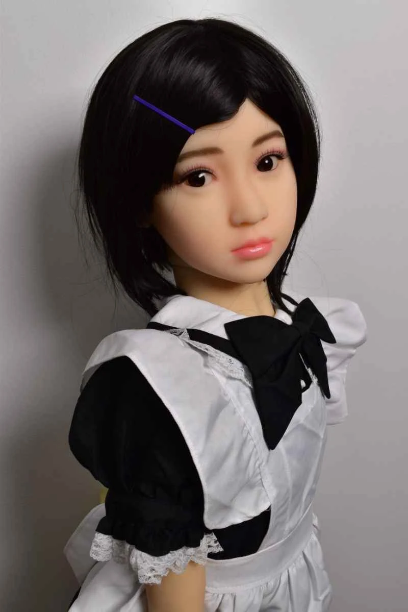
CATDOLL 128CM Katya Silicone Doll

Height: 128 Silicone Weight: 21kg Shoulder Width: 30cm Bust/Waist/Hip: 57/52/63cm Oral Depth: N/A Vaginal Depth: 3-15cm...

Articles 2026-02-22