Read next
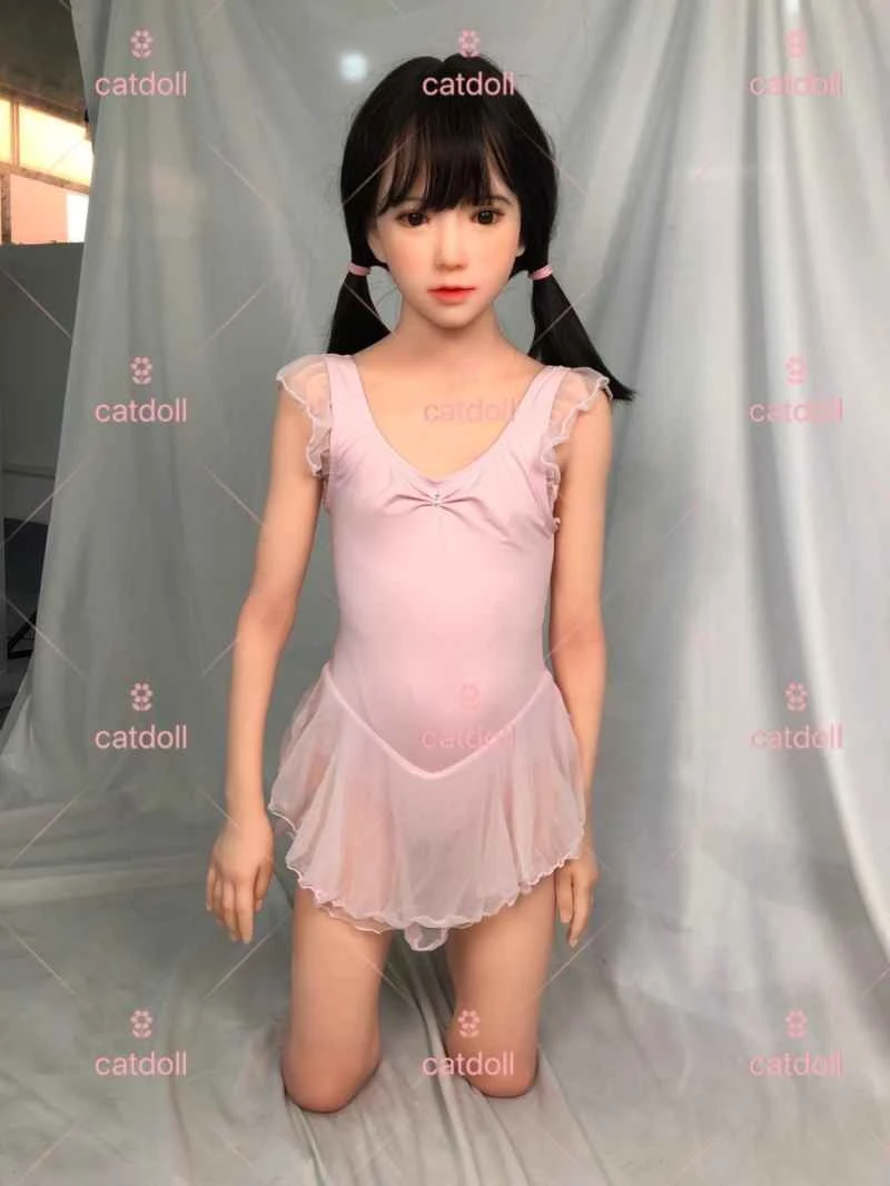
CATDOLL 139CM Luisa Silicone Doll
Height: 139 Silicone Weight: 25kg Shoulder Width: 33cm Bust/Waist/Hip: 61/56/69cm Oral Depth: N/A Vaginal Depth: 3-15cm...
Articles
2026-02-22
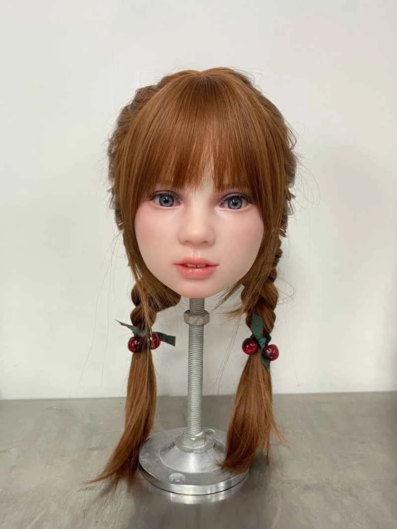
CATDOLL Katya Soft Silicone Head
Articles
2026-02-22
CATDOLL 135CM Tami
Articles
2026-02-22

Green lighting and intelligent lighting energy-saving control system
Articles
2026-02-22