Read next
CATDOLL Maruko 88CM TPE Doll
Height: 88cm Weight: 11.5kg Shoulder Width: 25cm Bust/Waist/Hip: 49/45/51cm Oral Depth: 3-5cm Vaginal Depth: 3-13cm Ana...
Articles
2026-02-22
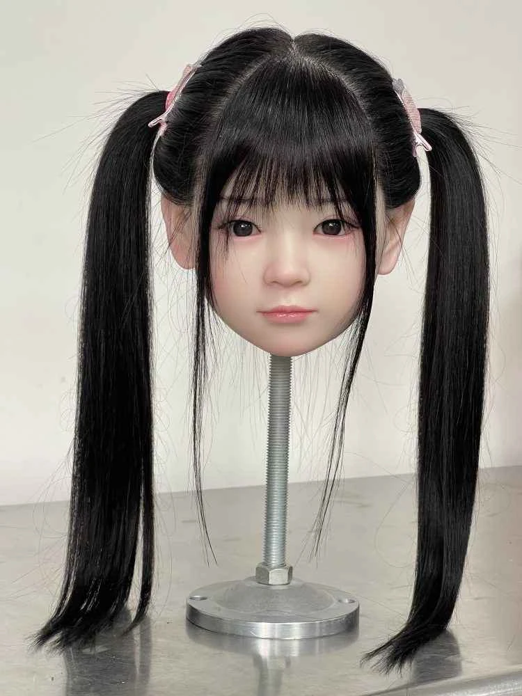
CATDOLL Cici Hard Silicone Head
Articles
2026-02-22

CATDOLL 128CM Cici Silicone Doll
Articles
2026-02-22

CATDOLL 115CM Kiki TPE
Articles
2026-02-22