Read next
Human-Machine Interface Prototyping Strategies for Embedded Systems
To simulate a human-machine interface (HMI) before the target hardware is completed, design engineers need to build an H...
Articles
2026-02-22

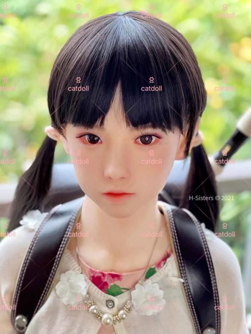
CATDOLL 115CM Nanako TPE
Articles
2026-02-22
CATDOLL 136CM Vivian (Customer Photos)
Articles
2026-02-22
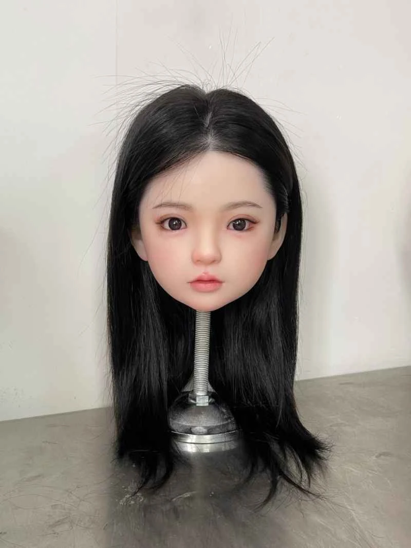
CATDOLL Dora Hard Silicone Head
Articles
2026-02-22