Read next
CATDOLL CATDOLL 115CM Dora (TPE Body with Soft Silicone Head)
Height: 115cm Weight: 19.5kg Shoulder Width: 29cm Bust/Waist/Hip: 57/53/64cm Oral Depth: 3-5cm Vaginal Depth: 3-15cm An...
Articles
2026-02-22
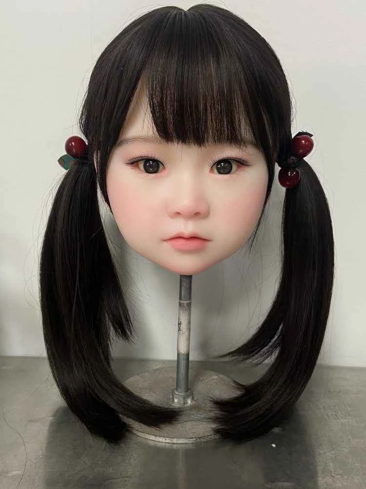
CATDOLL Momoko Soft Silicone Head
Articles
2026-02-22

CATDOLL 146CM Ya TPE (Customer Photos)
Articles
2026-02-22

CATDOLL 146CM B-CUP Tami (TPE Body with Hard Silicone Head) Customer Photos
Articles
2026-02-22