Read next
CATDOLL 108CM Coco
Height: 108cm Weight: 14.5kg Shoulder Width: 26cm Bust/Waist/Hip: 51/47/59cm Oral Depth: 3-5cm Vaginal Depth: 3-13cm An...
Articles
2026-02-22

CATDOLL 108CM Q Torso Doll
Articles
2026-02-22
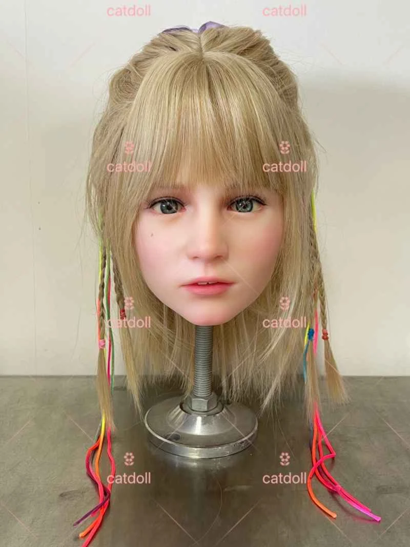
CATDOLL Oliva Soft Silicone Head
Articles
2026-02-22

CATDOLL 108CM Bebe Full Silicone Doll
Articles
2026-02-22