Read next
CATDOLL Oksana Soft Silicone Head
You can choose the skin tone, eye color, and wig, or upgrade to implanted hair. Soft silicone heads come with a functio...
Articles
2026-02-22
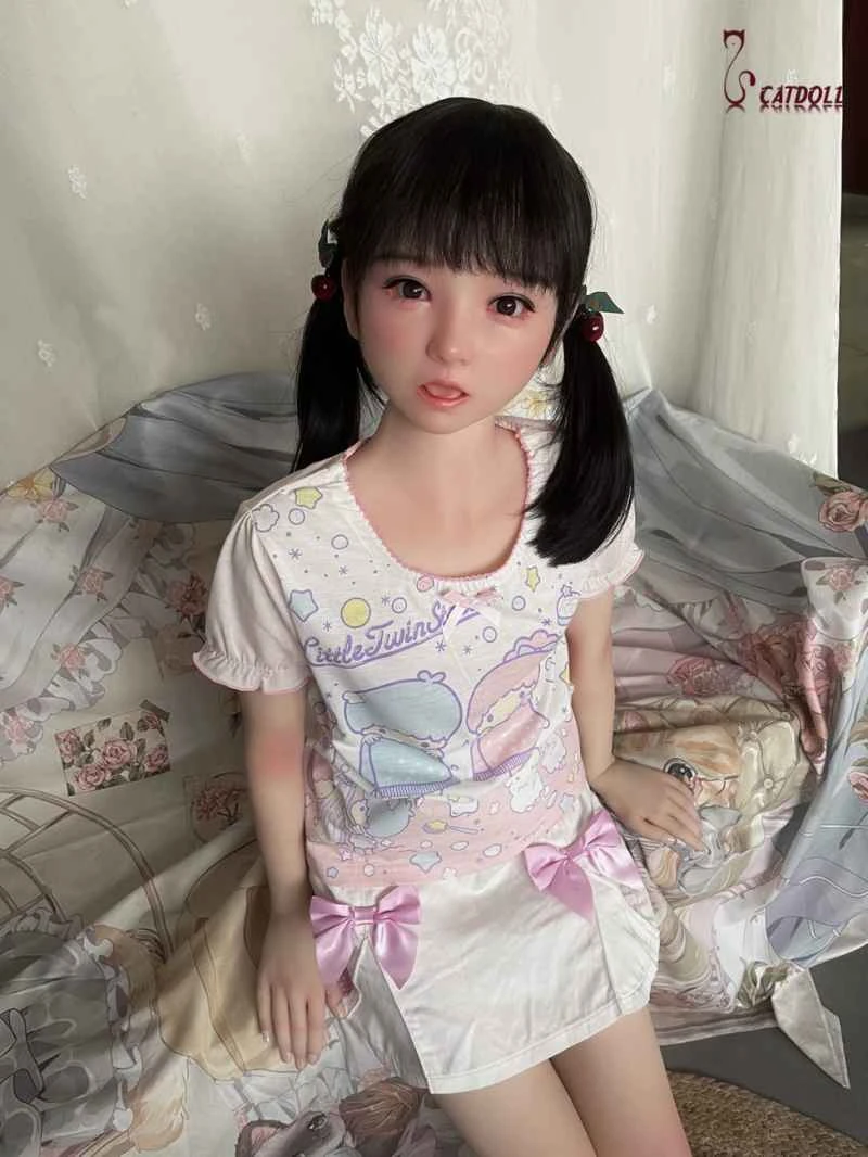
CATDOLL 138CM Yoyo (TPE Body with Soft Silicone Head)
Articles
2026-02-22

Measures for the sustainable development of concrete construction machinery
Articles
2026-02-22
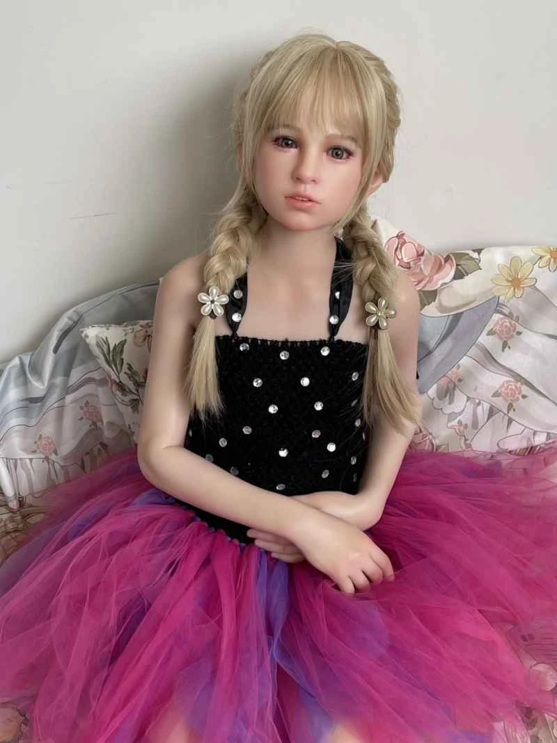
CATDOLL 128CM Dolly Silicone Doll
Articles
2026-02-22