Share this

70PR02 Programmable Logic Control Processing Module

2026-04-06 06:58:02 · · #1
0 Introduction The station control system of Gezhouba Converter Station adopts the ABB 70PR02 programmable logic controller module. This module is used to solve general control tasks and can also be used independently or coupled with other controllers and processors on the local bus. Data input and output are accomplished through the P13 local bus communication controller. Programming is done using the P10 functional language developed by ABB, which is simple and easy to learn. This module also has basic control application functions, and users can define their own combination functions. [b]1 Program Storage Process[/b] On the panel of the 70PR02 module, there is a PROGR key to insert the test memory 70SP02. It is used in conjunction with the programming box 70SK02 or 70SK03 to realize programming and debugging of user instruction lists, and can also read and modify instruction lists. Similarly, composite function instructions can also be modified and adjusted. 1.1 Instruction List The instruction list is the program written by the user. This program is written in P10 language. It includes the call of basic function blocks and composite function blocks. The memory storing these instruction lists consists of two parallel EPROMs. The storage range can be 2048 lines or 4096 lines, selected via jumper connector S41. The program ends with the instruction "END". If, for some reason, the instruction "END" is not processed within 120 ms, all outputs to the local bus are latched, an internal fault signal SME is generated, and the ALARM indicator is activated. 1.2 Composite Function List Composite function blocks are frequently used function blocks programmed by the user using the P10 language. They are called by the instruction list, and any number of composite function blocks can be stored in the program memory, as long as the memory capacity is not exceeded. However, only 64 composite function blocks (including repeated calls of a single composite function block) can be called in the instruction list. The storage capacity is 2048 lines or 4096 lines, selectable via jumper connector S42. The storage range (2048 lines or 4096 lines) for composite function instructions can be selected by the position of the S42 jumper connector. The program storage flow is shown in Figure 1. [align=center] Figure 1 Program Storage Flowchart[/align] [b]2 Program Processing Process[/b] The programming box 70SK03 or 70SK04 sends the user-written instructions to the storage unit of the 70PR02 module through the PROGR input port. After signal exchange, signal processing is performed. The processing part is composed of TTL-LS integrated circuits, with the core components being 28S42N and 18S130N type PROMs to implement this function. Its microprogrammer stores the processing instructions and service programs for basic functions. The processing part works with the data memory to process the instructions in the instruction list and composite function list in the program memory. 2.1 Program Processing Sequence The program is ready and can be started about 10 ms after the module is powered on. Initialization is required after startup under the following conditions: ① Power is switched on (US); ② The local bus address is disturbed; ③ When the module carries each test memory, the "RAM" or "PROM IN ACTION" button on it has been pressed, i.e., switching from EPROM to test memory. Initialization completes the following: All function blocks are initialized during the first approximately 35 cycles (700 ms). During this time and the following 10 cycles (200 ms), the module's output to the local bus is latched. 2.2 Input/Output Data Processing At the beginning of the processing cycle, data exchange is performed first. The number of data words exchanged can be adjusted by jumper connectors S21 to S32. The number of data words exchanged, i.e., the address of each data word, is 32, 64, and 128 respectively. After data exchange, the service routine is run. After the service routine is processed, the instruction list is processed until the "Program End" instruction (END) is completed. The function block "COED" performs the following functions: Records the pre-set "A0, A1" output by the module into bits 3 and 4 of the internal data storage field 00, and runs the "watchdog" program to make the processing cycle run continuously. After the function block "COED" finishes processing, the module's processing section will wait for the next new processing cycle. [b]3 Data Storage[/b] 3.1 Bus Data Storage Field The bus data storage field occupies 128 units of 16 bits; the address is 00~7F. In each processing cycle, local bus data is read through the local bus interface, and the processed data results are sent to the local bus. This is achieved by recognizing the information words of the traffic manager 70BV01 on the local bus through the interface. The processing section calls and stores data in the data storage area bit by bit using instructions with prefixes 4, 5, 8, and B. The functions of the four prefixes are as follows: 4 is a positive input, i.e., calling the serial data line DN; 5 is a negative input, i.e., calling the inverted serial data line DI; 8 and B are for storage. Data in this storage area can be indicated and simulated by the service device. 3.2 Internal Data Storage Area The internal data storage area occupies 128 units of 16-bit memory, with addresses 00 to 7F. For user programs, it serves as intermediate valid storage, and they are called bit-by-bit through the instruction table using instructions with prefixes 2, 3, and A. 3.3 Past Value Storage Area The past value storage area occupies 12 bits of memory. 1024 units store data for special functions, such as time-related or status input module data, which users cannot directly access. 3.4 Composite Function Internal Data Storage Area The composite function internal data storage area occupies 256 16-bit storage units, divided into 64 areas, each with 4 units. These 64 areas correspond to a maximum of 64 calls to composite function blocks, with each call allocating a new 4-unit area. The data in these storage units is accessed bit by bit by instructions in the composite function block with prefixes 2, 3, and A. The prefixes function as follows: 2 for positive access; 3 for negative access; and A for storing data in the storage unit. The address range is 00 to 03, with the highest address bit being F03. For example, to input the 6th bit (5 bits) in unit 01 within the composite function block, the instruction is: 2 501. [b]4 70PR02 Processing Module Interface with Local Bus[/b] The 70PR02 exchanges information with the local station bus via the serial address line AD, clock signal line CK, serial data line DN, and inverted serial data line DI. The standard voltage US supplied to the module is 24 V. 4.1 Local Bus Coupling Unit The coupling unit controls the data exchange between the module's data storage and the local bus. This unit includes a control system. This control system operates synchronously with the local bus. Data exchange with the local bus occurs for a short period at the beginning of each processing cycle. During this period, the control system of the coupling unit recognizes information from the local bus traffic manager 70BV01, receives data from the local bus and stores it in the bus data storage area, or sends the result of the previous processing cycle to the local bus. The management memory of the local bus coupling unit records the usage order of data in the instruction list, sequentially recording the usage of data words in the instruction list. Its two management bits indicate the usage status of the data word. For example, whether a certain data in the bus data storage area is a "source" (to be output to the local bus) or a "destination" (to be received from the local bus), or neither a "source" nor a "destination" (a unit that does not need to exchange data). During data exchange, this management bit memory is accessed. After determining the status of the data received on the local bus (data received after the control system recognizes the information) based on the information provided by the management bit, the local bus data is stored in the bus data storage area of ​​the data memory (see Table 1). When data is included in the instruction list, if the interference on the local bus exceeds 200 ms, the corresponding storage unit in the bus data storage area is set to 0000 and a fault signal SME is issued; if the interference does not exceed 200 ms, the storage unit will retain the previously stored correct data. 4.2 Analog Mode: The SIM key on the panel of the 70PR02 module allows insertion of auxiliary equipment for the debugging module of the analog memory 70SS01. During programming, signals received from the local bus or sent from the data storage to the local bus can be simulated through the analog interface SIM of the coupling unit. The analog memory 70SS01 is inserted into the SIM key on the panel. This memory can be connected to analog and indicator modules, such as 70SK02 and 70SK03, via a mutual cable. These indicator modules can perform the following functions: ① Indicating local bus signals; ② Simulating local bus input and output; ③ Tracking local bus signal interference or loss; ④ Indicating data in the internal storage. Internal data indication is handled by the service address. Data indicating a specific address is provided by the service address, while data signals can only be indicated by the analog interface. [b]5 Diagnosis[/b] When a module malfunctions, it outputs the hardware signals SME, SMS, and SMG, and issues an alarm signal. 5.1 SME Alarm Signal SME alarm signals indicate internal electronic interference. These signals are generated by the module's monitoring unit. The causes and consequences of these signals are as follows: First cause: Address transmission is interfered with; the RAM or PROM button of the test memory 70SP02 is activated. If the alarm signal is caused by either of these two reasons, the logic controller will be cleared and the output of the local bus will be locked. After these interferences disappear, the device will be restarted with initialization. Second cause: The program cannot be completed in the instruction list because the instruction "END" is lost; the program is too long; the processing order is interfered with. If the alarm signal is caused by these reasons, the logic control will be locked to the output of the local bus for the next 120 ms. The third reason: The data input to the local bus is interfered with, or the loss time exceeds 200 ms. If this is the case, after 200 ms, the storage unit of the data memory corresponding to the lost data is set to 0000. If all data transmitted on the local bus is correct and valid again, the fault indication signal will disappear. The fourth reason: The internal power supply voltage is too high; the data has not been delivered after more than 120 ms from the local bus to the data storage. In this case, only an alarm is triggered. 5.2 SMS Analog Signal If the signal of the local bus is simulated by the analog memory 70SS01, an SMS signal will appear and disappear until the analog status signal does not appear. 5.3 SMG Device Fault Signal The SMG signal is a combination of the SME signal and the SMS signal. [b]6 Conclusion[/b] The above is an analysis of the 70PR02 programmable logic control module. The operation mode of this module is flexible and adjustable, such as the maximum processing time and program length are adjustable. This module has the following basic functions: ① Logic operations: AND gate, OR gate, RS bistable; ② Timing elements: delayed start, delayed return; ③ Decrement of counter reading; ④ Signal comparison: 3-out-of-2, 4-out-of-2; ⑤ Multifunctionality: sequential function, pre-selection function. Edited by: He Shiping
Read next

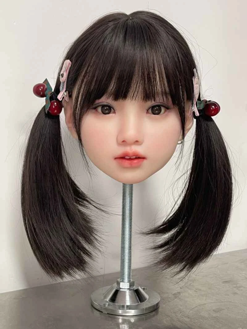
CATDOLL Yana Hybrid Silicone Head

The hybrid silicone head is crafted using a soft silicone base combined with a reinforced scalp section, allowing durab...

Articles 2026-02-22