Read next
Discussion on the Integration and Upgrading of DCS Control Systems
1. Process Status and Automation System Background of Nantong Acetate Fiber Co., Ltd. Nantong Acetate Fiber Co., Ltd. (h...
Articles
2026-02-22

CATDOLL 108CM Dodo – Customer Photos
Articles
2026-02-22
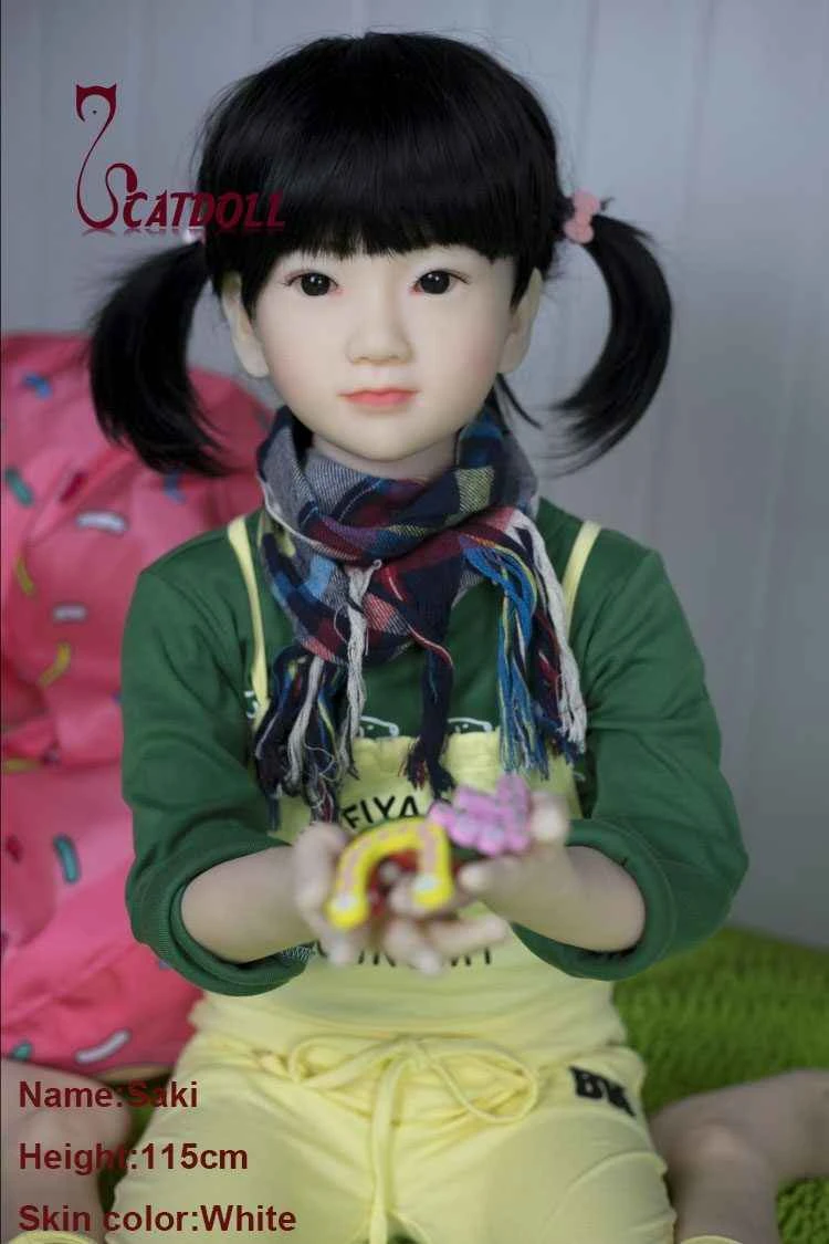
CATDOLL CATDOLL 115CM Saki TPE
Articles
2026-02-22

CATDOLL 133CM Sasha Shota Doll
Articles
2026-02-22