Read next
CATDOLL Christina Hard Silicone Head
The head made from hard silicone does not have a usable oral cavity. You can choose the skin tone, eye color, and wig, ...
Articles
2026-02-22

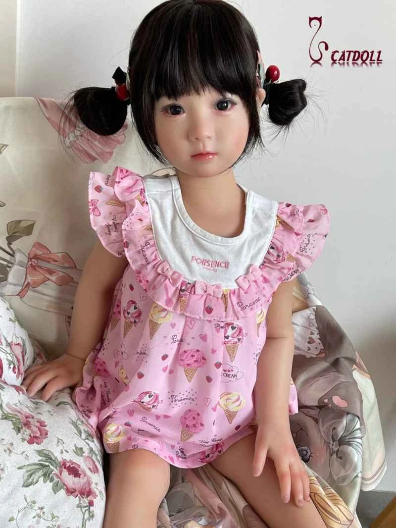
CATDOLL 135CM Tami
Articles
2026-02-22

Digital technology of power isolation sensors
Articles
2026-02-22
CATDOLL 88CM Q Full Silicone Doll
Articles
2026-02-22