Read next
CATDOLL 148CM Sana (TPE Body with Hard Silicone Head)
Height: 148cm Weight: 30kg Shoulder Width: 34cm Bust/Waist/Hip: 70/58/82cm Oral Depth: 3-5cm Vaginal Depth: 3-15cm Anal...
Articles
2026-02-22

CATDOLL 139CM Luisa Silicone Doll
Articles
2026-02-22
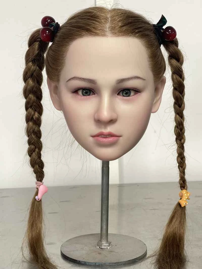
CATDOLL Christina Hard Silicone Head
Articles
2026-02-22

CATDOLL CATDOLL 115CM Milan (TPE Body with Hard Silicone Head)
Articles
2026-02-22