Read next
CATDOLL 148CM Christina Silicone Doll
Height: 148 Silicone Weight: 33kg Shoulder Width: 34cm Bust/Waist/Hip: 70/58/82cm Oral Depth: N/A Vaginal Depth: 3-15cm...
Articles
2026-02-22
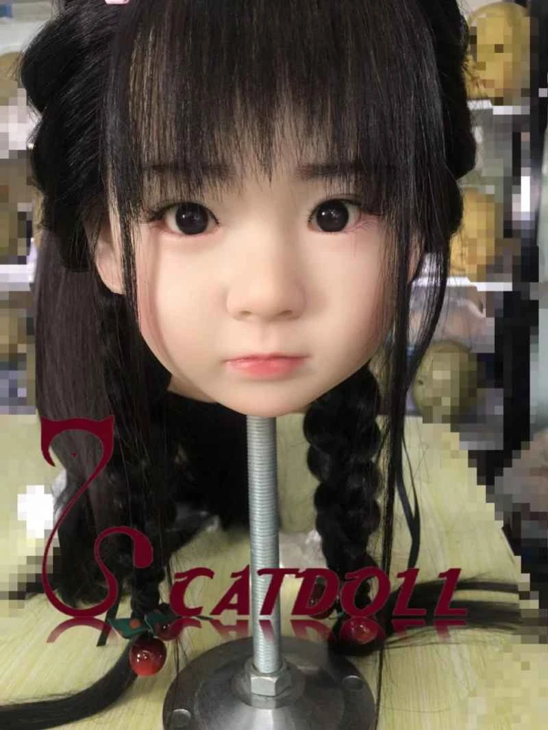
CATDOLL Cici Hard Silicone Head
Articles
2026-02-22
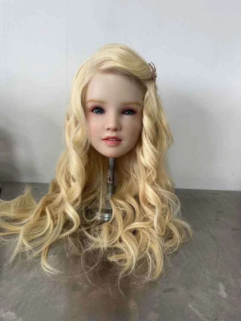
CATDOLL Kelsie Hard Silicone Head
Articles
2026-02-22
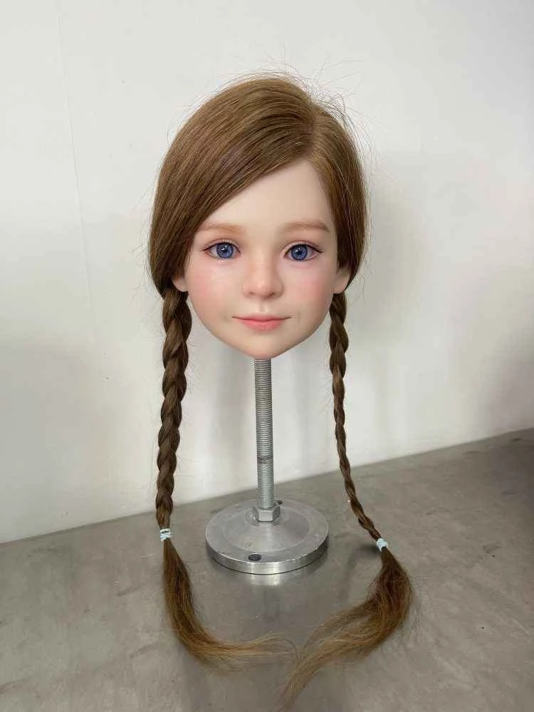
CATDOLL Rosie Hard Silicone Head
Articles
2026-02-22