Read next
CATDOLL 136CM Ya (TPE Body with Hard Silicone Head)
Height: 136cm Weight: 23.3kg Shoulder Width: 31cm Bust/Waist/Hip: 60/54/68cm Oral Depth: 3-5cm Vaginal Depth: 3-15cm An...
Articles
2026-02-22
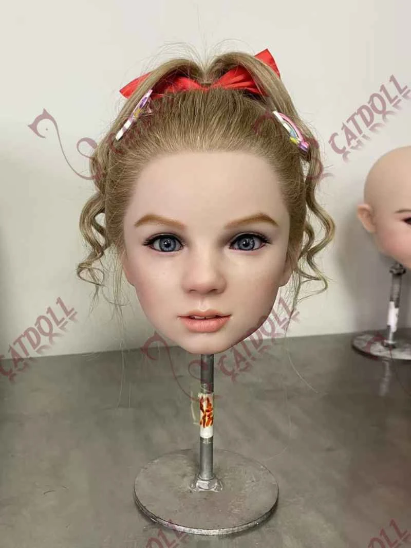
CATDOLL Katya Hybrid Silicone Head
Articles
2026-02-22

Power Electronics and Power Management
Articles
2026-02-22
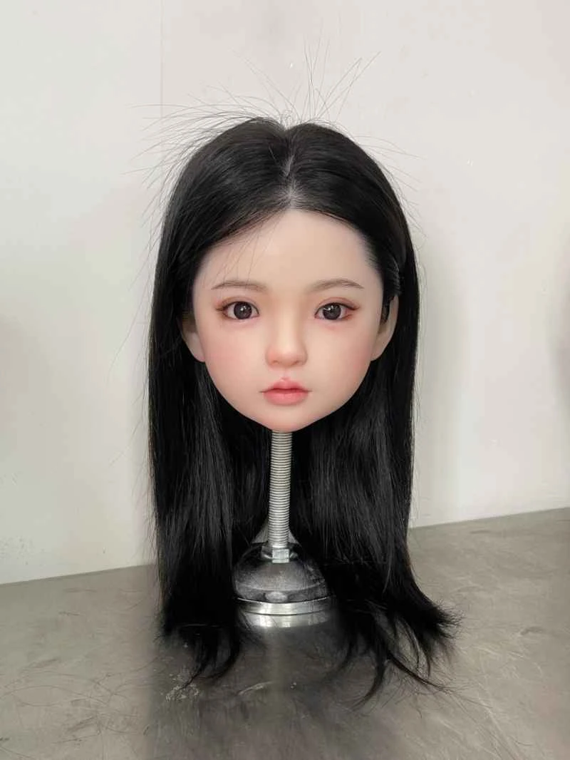
CATDOLL Dora Hard Silicone Head
Articles
2026-02-22