Read next
CATDOLL 150CM Sana Mini TPE Doll
Height: 150cm Weight: 36kg Shoulder Width: 36cm Bust/Waist/Hip: 73/64/85cm Oral Depth: 3-5cm Vaginal Depth: 3-15cm Anal...
Articles
2026-02-22
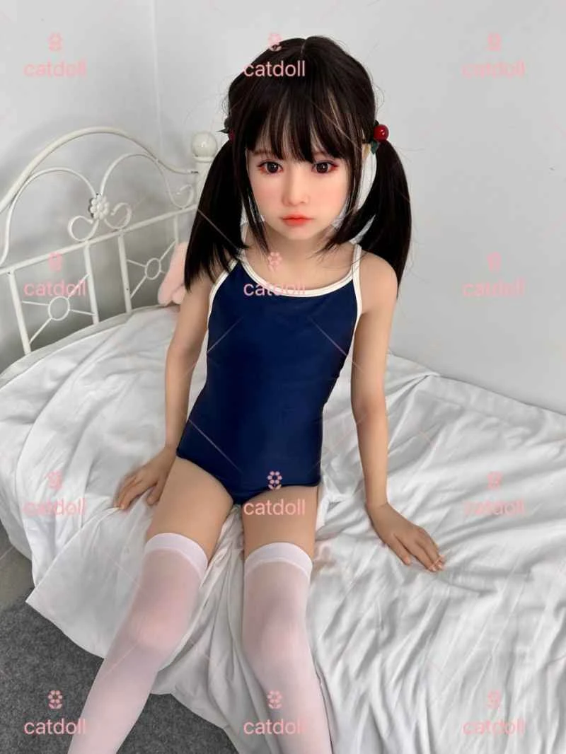
CATDOLL 128CM Yuki
Articles
2026-02-22
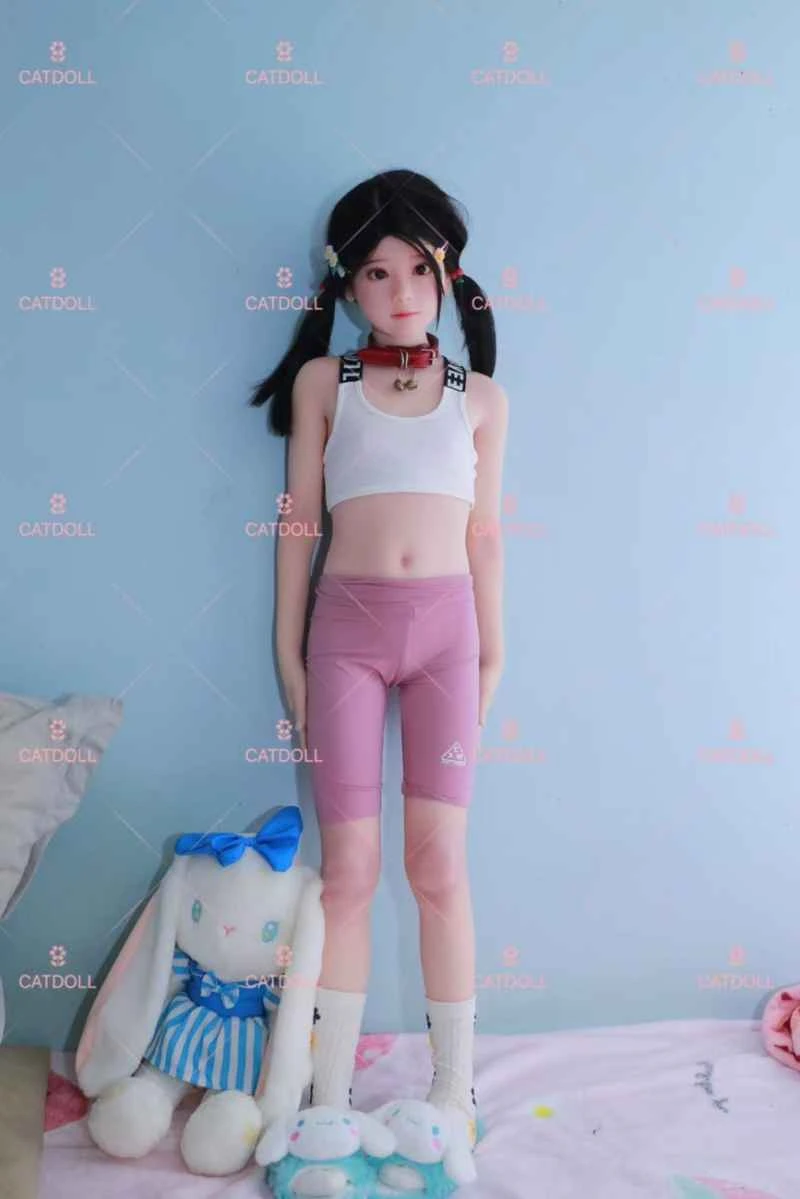
CATDOLL 128CM Cici (Customer Photos)
Articles
2026-02-22
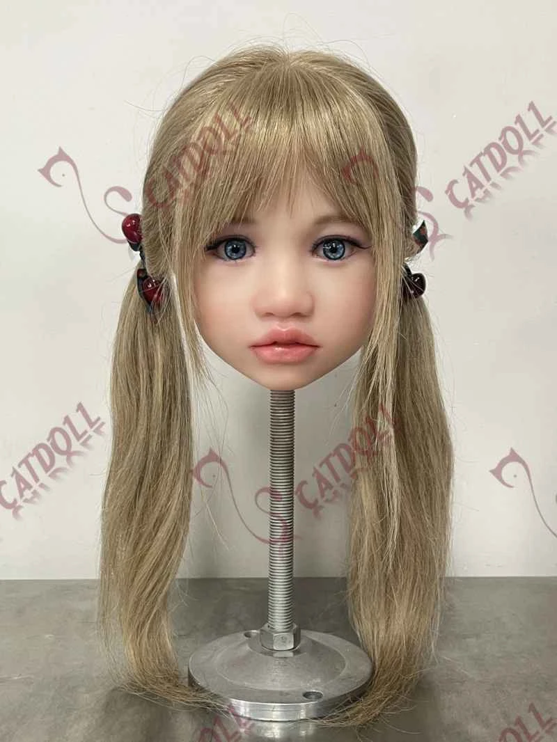
CATDOLL Sabrina Hybrid Silicone Head
Articles
2026-02-22