Read next
CATDOLL 138CM Tami Torso Doll
Height: 138 Torso Weight: 18.5kg Shoulder Width: 30cm Bust/Waist/Hip: 64/59/74cm Oral Depth: 3-5cm Vaginal Depth: 3-15c...
Articles
2026-02-22
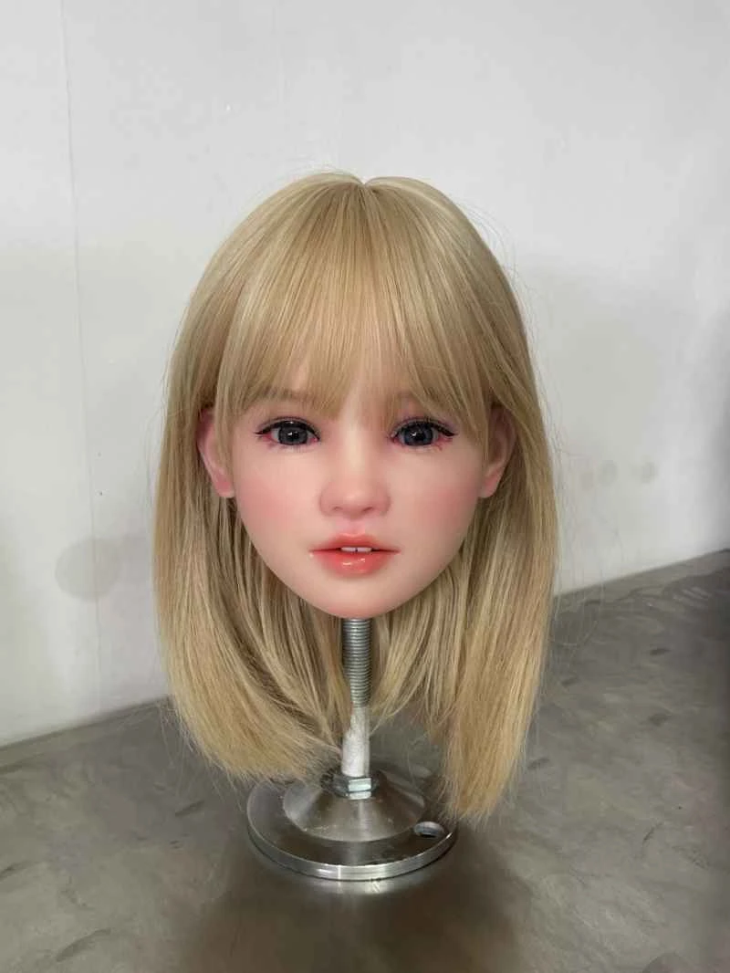
CATDOLL Kelsie Soft Silicone Head
Articles
2026-02-22

Implementation of BACnet-MS/TP protocol stack in embedded systems
Articles
2026-02-22

CATDOLL 123CM Sasha TPE
Articles
2026-02-22