Read next
CATDOLL 102CM Ling Anime Doll
Height: 102cm Weight: 15.5kg Shoulder Width: 26cm Bust/Waist/Hip: 51/46/66cm Oral Depth: 3-5cm Vaginal Depth: 3-13cm An...
Articles
2026-02-22
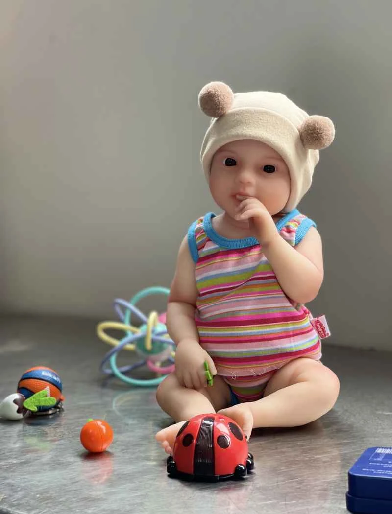
CATDOLL 42CM TPE Baby Doll
Articles
2026-02-22
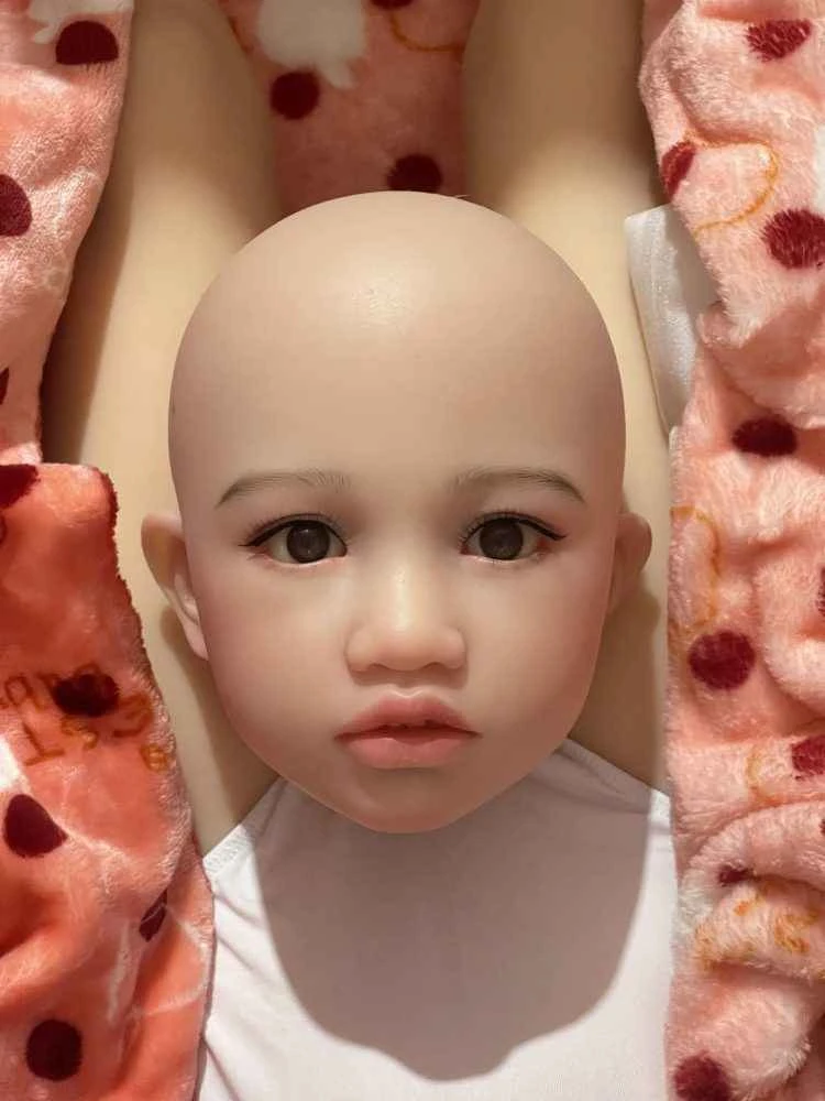
CATDOLL Sabrina Soft Silicone Head
Articles
2026-02-22
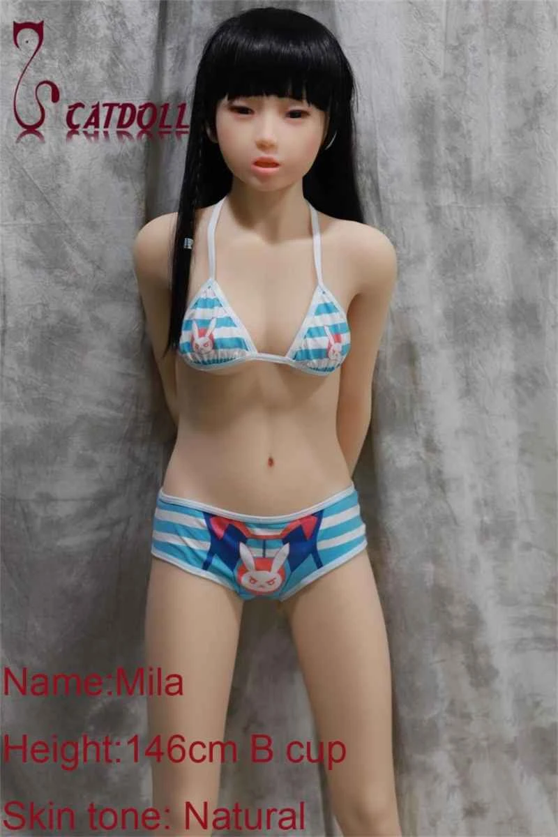
CATDOLL 146CM Mila TPE
Articles
2026-02-22