Share this

Gigabit Ethernet Interface Design Based on MPC8560

2026-04-06 06:14:33 · · #1
With the development of network technology, the application of network communication controllers has become increasingly widespread. The MPC8560 PowerQUICC III, integrating a PowerPC microprocessor, is a versatile, high-performance communication microprocessor with a highly flexible integrated unit system and peripheral communication controllers. It can be widely used in communication and network systems and is one of the most advanced integrated communication microprocessors designed for the telecommunications and network markets. It integrates a rich set of network and communication peripherals, providing greater flexibility, scalability, and higher integration. MPC8560 Introduction: The MPC8560 integrates two processing modules: a high-performance embedded PowerPC e500 core and a communication processing module (CPM). In addition, the chip provides on-chip cache, DDR controller, programmable interrupt controller, general-purpose I/O ports, DMA, and I2C interface controllers. The biggest difference between the MPC8560 and the more commonly used MPC8260 is that the MPC8560 adds two Three-Speed ​​Ethernet Controllers (TSEC), implementing Ethernet protocol interface control at three different speeds: 10Mb/s, 100Mb/s, and 1Gb/s. This article will primarily discuss how to implement Gigabit Ethernet interfaces using these two TSECs. Gigabit Ethernet Physical Layer Protocols and Interfaces References often limit introductions to network protocols to theoretical analyses of protocol layering, with limited discussion of interfaces in practical applications, especially for Gigabit Ethernet. This article will provide a summary overview of the interfaces used in Gigabit Ethernet applications. The data link layer of the Gigabit Ethernet protocol is the same as the traditional 10/100Mb/s Ethernet protocol, but the physical layer differs. The correspondence between the three protocols and the OSI seven-layer model is shown in Figure 1. Figure 1: Correspondence between the three Ethernet protocols and the OSI model. As can be seen from Figure 1, the difference between the Gigabit Ethernet protocol and the 10/100Mb/s Ethernet protocol lies solely in the physical layer. In the diagram, PHY represents the chip implementing the physical layer protocol; the reconciliation sublayer is used for instruction translation; MII (Media Independent Interface)/GMII (Gigabit Media Independent Interface) is the interface between the physical layer chip and the chip implementing the upper-layer protocol; MDI (Media Dependent Interface) is the interface between the physical layer chip and the physical medium; PCS, PMA, and PMD represent the respective sublayers implementing the physical layer protocol. In practical application systems, the operational details of these sublayers are all implemented by the PHY chip; only the design and operation of the MII and MDI interfaces need to be addressed. There are four main physical layer interface standards for Gigabit Ethernet: GMII, RGMII (Reduced GMII), TBI (Ten-Bit Interface), and RTBI (Reduced TBI). GMII is the standard Gigabit Ethernet interface, located between the MAC layer and the physical layer. For the TBI interface, the functions of the PCS sublayer in Figure 1 are implemented by the MAC layer chip, reducing the complexity of the PHY chip and requiring fewer control lines than the GMII interface. Both GMII and RTBI interfaces double the transmission rate per data line while halving the number of data lines. Therefore, using the TBI interface to implement a Gigabit Ethernet interface requires fewer control and data lines than the GMII interface, making design and use relatively easier. Although the TBI interface has more data lines than the RTBI interface, the transmission rate per data line can be half, significantly reducing PCB layout complexity. Therefore, compared to other methods, using the TBI interface is the simplest and least difficult to implement. Furthermore, TBI interface PHY chips are much cheaper than GMII interface PHY chips. For chips that provide both GMII and TBI interfaces, the TBI interface design is recommended. MPC8560 Interface Design with PHY Chip: The MPC8560 supports four different interface standards; this article only discusses the TBI interface. The TLK2201 chip is a single-channel Gigabit Ethernet transceiver that supports both TBI and RTBI interfaces. It is among the industry's first 2.5V devices compliant with the 802.3 specification, requiring no external capacitors. This saves board space, reduces the number of components, and lowers product costs. Furthermore, the chip boasts remarkably low power consumption. Figure 2 shows the interface design between the MPC8560 and TLK2201. It's important to note that TD0-TD9 and RD0-RD9 are not all data lines. TD8 corresponds to Tx_ER, serving as a transmit error flag; TD9 corresponds to Tx_EN, serving as a transmit enable bit; RD8 corresponds to Rx_DV, serving as a receive data valid bit; and RD9 corresponds to Rx_ER, serving as a receive error detection bit. It should also be noted that an SFP (pluggable) optical module is used in the diagram because the TLK2201 only provides a gigabit Ethernet interface for the optical module. The initialization process for the MPC8560's TSEC controller is as follows. By following the steps sequentially, the gigabit network interface of the TSEC can be correctly configured. Configure the MACCFG1 register to perform a soft reset of the MAC; clear the soft reset of the MACCFG1 register; configure the MACCFG2 register to select the TSEC operating mode (e.g., full-duplex or half-duplex, CRC check enabled, etc.); initialize the ECNTRL register and set the interface to the TBI standard; set the MAC address and physical address; set the MII port speed and initialize the PHY using MDIO; clear and set the interrupt-related registers IEVENT and IMASK; set the hash table and hash register; initialize the receive control register RCTRL; set the DMA control register DMATRL; set the receive buffer size; set the transmit/receive buffer descriptor (BD); set the transmit/receive enable bit in MACCFG1 to complete the TSEC initialization. During TSEC initialization, it is particularly important to note that after setting the registers, the controller is in an unstable state and cannot immediately execute the next operation; a certain delay is required. Typically, the corresponding status register can be read to determine if the next step can proceed, or a timer delay provided by some operating systems can be used, such as taskDelay() in VxWorks. Testing and Results To test the performance of the designed Gigabit Ethernet interface, it was connected to SmartBits, a dedicated instrument for testing network interface performance. A simple test method involves using SmartBits to send data packets to the MPC8560's Gigabit Ethernet interface. Upon receiving the packets, the MPC8560 directly returns the data to SmartBits. SmartBits then compiles and displays the test results. Figure 3 shows the Gigabit Ethernet interface test results. The transmission rate (Rates) can reach approximately 1Gb/s, with a slight margin. To test the more comprehensive performance of the Gigabit Ethernet interface, tests with different sized data packets and bursts of large data streams are necessary. Due to space limitations, specific test details will not be discussed further. Design Considerations Due to the relatively high transmission rate on the data lines, the hardware design needs to consider the following points: The transmission rate of each data line in the TBI interface is 125Mb/s. To ensure sampling and signal synchronization, the lengths of the receive signal lines RD0-RD9 and the receive clock line RxCLK must be equal. Similarly, the lengths of the transmit signal lines TD0 to TD9 and the transmit clock line TxCLK must be equal. To ensure impedance matching, the impedance of all signal lines in the TBI interface must be controlled within 50Ω ± 5%. The input signal of the optical module is a high-speed differential signal; therefore, the design should ensure that the two pairs of differential signal lines for receiving and transmitting are of equal length. Simultaneously, the differential impedance needs to be controlled within 100Ω ± 5% to ensure impedance matching. To ensure clean power supply, a filter must be added to the PLL power input of the TLK2201. The following points should be considered in the design of the driver software: GE port transceiver requires high software processing capabilities; therefore, the depth of the transmit/receive buffer needs to be carefully designed, and the transmit/receive processing program should be reasonably scheduled to ensure data transmission and reception performance. For the maintenance of the BD table, the BD read/write pointers and the BD status flags need to be correctly maintained to avoid buffer overlap and overflow. In particular, the BD read/write pointers should cycle at appropriate positions according to the size of the transmit/receive buffers. If the PHY is configured to use auto-negotiation, you must ensure that auto-negotiation is working properly before you can configure the TSEC to use full-duplex or half-duplex mode.
Read next

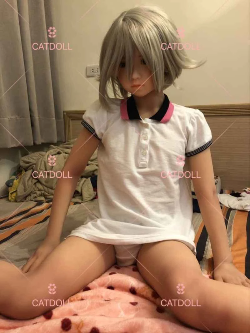
CATDOLL 88CM Q Full Silicone Doll

Height: 88cm Silicone Weight: 14kg Shoulder Width: 25cm Bust/Waist/Hip: 49/45/51cm Oral Depth: N/A Vaginal Depth: 3-13c...

Articles 2026-02-22