Read next
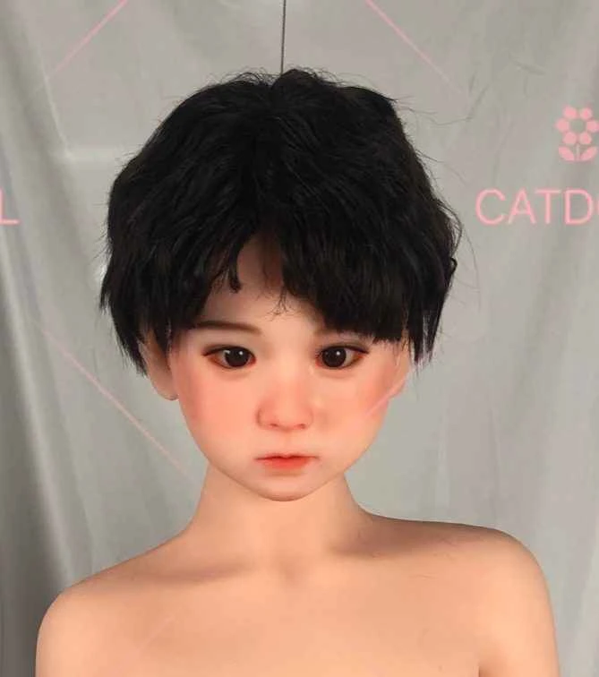
CATDOLL Q Soft Silicone Head
You can choose the skin tone, eye color, and wig, or upgrade to implanted hair. Soft silicone heads come with a functio...
Articles
2026-02-22
CATDOLL 133CM Kiki Shota Doll
Articles
2026-02-22
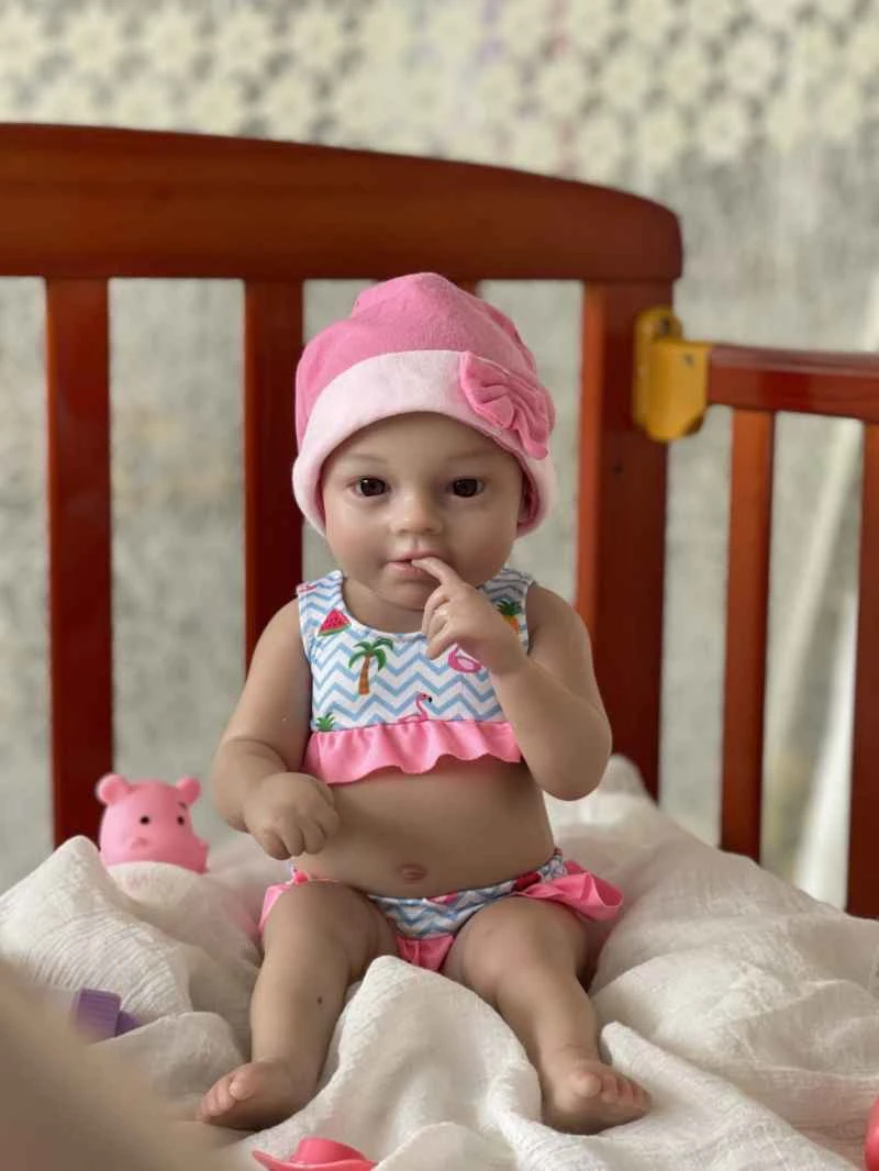
CATDOLL 42CM Silicone Reborn Baby Doll
Articles
2026-02-22

CAN Interface Design of Smart Instruments
Articles
2026-02-22