Read next
CATDOLL 139CM Sasha Silicone Doll
Height: 139 Silicone Weight: 25kg Shoulder Width: 33cm Bust/Waist/Hip: 61/56/69cm Oral Depth: N/A Vaginal Depth: 3-15cm...
Articles
2026-02-22

CATDOLL 138CM Airi(TPE Body with Hard Silicone Head)
Articles
2026-02-22
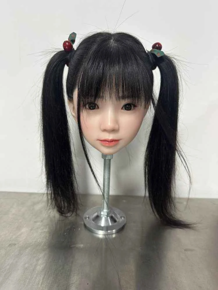
CATDOLL Himari Hard Silicone Head
Articles
2026-02-22
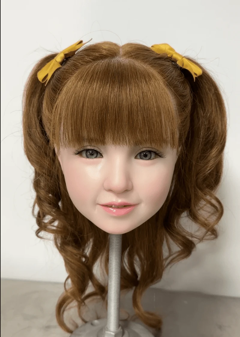
CATDOLL Oksana Hard Silicone Head
Articles
2026-02-22