Read next
CATDOLL 128CM Kiki (TPE Body with Hard Silicone Head)
Height: 128cm Weight: 19kg Shoulder Width: 30cm Bust/Waist/Hip: 57/52/63cm Oral Depth: 3-5cm Vaginal Depth: 3-15cm Anal...
Articles
2026-02-22

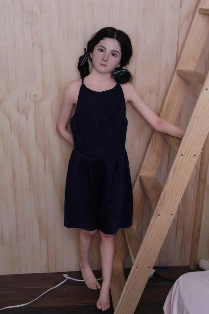
CATDOLL 123CM Ava (TPE Body with Hard Silicone Head)
Articles
2026-02-22

CATDOLL Kara Hard Silicone Head
Articles
2026-02-22
CATDOLL 135CM Lucy(TPE Body with Hard Silicone Head)
Articles
2026-02-22